CMOS
a
12-Bit Monolithic Multiplying DAC
AD7541A
FEATURES
FUNCTIONAL BLOCK DIAGRAM
Improved Version of AD7541
Full Four-Quadrant Multiplication
12-Bit Linearity (Endpoint)
All Parts Guaranteed Monotonic
TTL/CMOS Compatible
10kΩ
10kΩ
10kΩ
V
REF
20kΩ
20kΩ
S2
20kΩ
20kΩ
20kΩ
S1
S3
S12
Low Cost
Protection Schottky Diodes Not Required
Low Logic Input Leakage
OUT2
OUT1
10kΩ
R
FEEDBACK
GENERAL DESCRIPTION
BIT 1 (MSB)
BIT 2
BIT 3
BIT 12 (LSB)
The Analog Devices AD7541A is a low cost, high performance
12-bit monolithic multiplying digital-to-analog converter. It is
fabricated using advanced, low noise, thin film on CMOS
technology and is available in a standard 18-lead DIP and in
20-terminal surface mount packages.
DIGITAL INPUTS (DTL/TTL/CMOS COMPATIBLE)
LOGIC: A SWITCH IS CLOSED TO I
FOR
OUT1
ITS DIGITAL INPUT IN A "HIGH" STATE.
PRODUCT HIGHLIGHTS
Compatibility: The AD7541A can be used as a direct replace-
ment for any AD7541-type device. As with the Analog Devices
AD7541, the digital inputs are TTL/CMOS compatible and
have been designed to have a ±1 µA maximum input current
requirement so as not to load the driving circuitry.
The AD7541A is functionally and pin compatible with the in-
dustry standard AD7541 device and offers improved specifica-
tions and performance. The improved design ensures that the
device is latch-up free so no output protection Schottky diodes
are required.
Improvements: The AD7541A offers the following improved
specifications over the AD7541:
This new device uses laser wafer trimming to provide full 12-bit
endpoint linearity with several new high performance grades.
1. Gain Error for all grades has been reduced with premium
ORDERING GUIDE1
grade versions having a maximum gain error of ±3 LSB.
2. Gain Error temperature coefficient has been reduced to
Relative
Gain
Error
2 ppm/°C typical and 5 ppm/°C maximum.
Temperature
Range
Accuracy
Package
Model2
TMIN to TMAX TA = +25؇C Options3
3. Digital-to-analog charge injection energy for this new device
is typically 20% less than the standard AD7541 part.
AD7541AJN 0°C to +70°C
AD7541AKN 0°C to +70°C
±1 LSB
±1/2 LSB
±1 LSB
±1/2 LSB
±1/2 LSB
±1 LSB
±6 LSB
±1 LSB
±6
±1
±1
±6 LSB
±1 LSB
±6 LSB
±1 LSB
±6 LSB
±1 LSB
N-18
N-18
P-20A
P-20A
R-18
Q-18
Q-18
Q-18
Q-18
E-20A
E-20A
4. Latch-up proof.
AD7541AJP
0°C to +70°C
AD7541AKP 0°C to +70°C
AD7541AKR 0°C to +70°C
AD7541AAQ –25°C to +85°C
AD7541ABQ –25°C to +85°C
5. Improvements in laser wafer trimming provides 1/2 LSB max
differential nonlinearity for top grade devices over the operat-
ing temperature range (vs. 1 LSB on older 7541 types).
±1/2 LSB
AD7541ASQ –55°C to +125°C ±1 LSB
AD7541ATQ –55°C to +125°C ±1/2 LSB
AD7541ASE –55°C to +125°C ±1 LSB
AD7541ATE –55°C to +125°C ±1/2 LSB
6. All grades are guaranteed monotonic to 12 bits over the
operating temperature range.
NOTES
1Analog Devices reserves the right to ship either ceramic (D-18) or cerdip (Q-18)
hermetic packages.
2To order MIL-STD-883, Class B process parts, add /883B to part number. Contact
local sales office for military data sheet.
3E = Leadless Ceramic Chip Carrier; N = Plastic DIP; P = Plastic Leaded Chip
Carrier; Q = Cerdip; R = Small Outline IC.
REV. B
Information furnished by Analog Devices is believed to be accurate and
reliable. However, no responsibility is assumed by Analog Devices for its
use, nor for any infringements of patents or other rights of third parties
which may result from its use. No license is granted by implication or
otherwise under any patent or patent rights of Analog Devices.
One Technology Way, P.O. Box 9106, Norwood, MA 02062-9106, U.S.A.
Tel: 617/329-4700
Fax: 617/326-8703
World Wide Web Site: http://www.analog.com
© Analog Devices, Inc., 1997


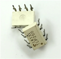
 TLP250光耦合器:资料手册参数分析

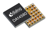
 DA14580 低功耗蓝牙系统级芯片(SoC):资料手册参数分析

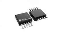
 INA226 高精度电流和功率监控器:资料手册参数分析

 SI2302 N沟道MOSFET:资料手册参数分析
