
 5秒后页面跳转

| 是否无铅: | 含铅 | 是否Rohs认证: | 符合 |
| 生命周期: | Obsolete | 零件包装代码: | SOIC |
| 包装说明: | SOP, SOP20,.4 | 针数: | 20 |
| Reach Compliance Code: | unknown | ECCN代码: | EAR99 |
| HTS代码: | 8542.39.00.01 | 风险等级: | 5.07 |
| JESD-30 代码: | R-PDSO-G20 | JESD-609代码: | e3 |
| 长度: | 12.8 mm | 湿度敏感等级: | 1 |
| 功能数量: | 1 | 端子数量: | 20 |
| 最高工作温度: | 105 °C | 最低工作温度: | -40 °C |
| 封装主体材料: | PLASTIC/EPOXY | 封装代码: | SOP |
| 封装等效代码: | SOP20,.4 | 封装形状: | RECTANGULAR |
| 封装形式: | SMALL OUTLINE | 峰值回流温度(摄氏度): | 260 |
| 电源: | 3 V | 认证状态: | Not Qualified |
| 座面最大高度: | 2.65 mm | 子类别: | Modems |
| 最大压摆率: | 0.0125 mA | 标称供电电压: | 3 V |
| 表面贴装: | YES | 技术: | CMOS |
| 电信集成电路类型: | TELECOM CIRCUIT | 温度等级: | INDUSTRIAL |
| 端子面层: | Matte Tin (Sn) | 端子形式: | GULL WING |
| 端子节距: | 1.27 mm | 端子位置: | DUAL |
| 处于峰值回流温度下的最长时间: | 40 | 宽度: | 7.5 mm |
| Base Number Matches: | 1 |
| 型号 | 品牌 | 描述 | 获取价格 | 数据表 |
| AD73311LAR | ADI | Low Cost, Low Power CMOS General Purpose Analog Front End |
获取价格 |

|
| AD73311LAR-REEL | ADI | 暂无描述 |
获取价格 |
|
| AD73311LAR-REEL7 | ADI | IC SPECIALTY TELECOM CIRCUIT, PDSO20, 0.300 INCH, SOIC-20, Telecom IC:Other |
获取价格 |
|
| AD73311LARS | ADI | Low Cost, Low Power CMOS General Purpose Analog Front End |
获取价格 |
|
| AD73311LARS-REEL | ADI | 暂无描述 |
获取价格 |
|
| AD73311LARS-REEL7 | ADI | IC SPECIALTY TELECOM CIRCUIT, PDSO20, SSOP-20, Telecom IC:Other |
获取价格 |
|
 CC2530无线微控制器:资料手册参数分析

 NE5532双低噪声运算放大器:资料手册参数分析
 74LS138 3-to-8线解码器/多路复用器:资料手册参数分析
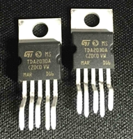 TDA2030音频功率放大器:资料手册参数分析
工作时间:9:00-21:00
CEO邮箱:ceo@jiepei.com
投诉邮箱:tousu@jiepei.com


 浙公网安备 33010502006866号 浙ICP备10014259号-119
营业执照ICP证
浙公网安备 33010502006866号 浙ICP备10014259号-119
营业执照ICP证


