
 5秒后页面跳转

| 是否无铅: | 不含铅 | 是否Rohs认证: | 符合 |
| 生命周期: | Active | 零件包装代码: | SOIC |
| 包装说明: | SOP, | 针数: | 8 |
| Reach Compliance Code: | unknown | 风险等级: | 5.14 |
| 放大器类型: | OPERATIONAL AMPLIFIER | 标称共模抑制比: | 96 dB |
| 最大输入失调电压: | 1000 µV | JESD-30 代码: | R-PDSO-G8 |
| JESD-609代码: | e3 | 长度: | 4.9 mm |
| 湿度敏感等级: | 1 | 负供电电压上限: | -18 V |
| 标称负供电电压 (Vsup): | -15 V | 功能数量: | 1 |
| 端子数量: | 8 | 最高工作温度: | 85 °C |
| 最低工作温度: | -40 °C | 封装主体材料: | PLASTIC/EPOXY |
| 封装代码: | SOP | 封装形状: | RECTANGULAR |
| 封装形式: | SMALL OUTLINE | 峰值回流温度(摄氏度): | 260 |
| 座面最大高度: | 1.75 mm | 标称压摆率: | 2.1 V/us |
| 子类别: | Operational Amplifier | 供电电压上限: | 18 V |
| 标称供电电压 (Vsup): | 15 V | 表面贴装: | YES |
| 温度等级: | INDUSTRIAL | 端子面层: | MATTE TIN |
| 端子形式: | GULL WING | 端子节距: | 1.27 mm |
| 端子位置: | DUAL | 处于峰值回流温度下的最长时间: | 40 |
| 宽度: | 3.9 mm | Base Number Matches: | 1 |
| 型号 | 品牌 | 替代类型 | 描述 | 数据表 |
| AD629BRZ-RL | ADI |
类似代替  |
High Common-Mode Voltage, Difference Amplifier |

|
| 型号 | 品牌 | 获取价格 | 描述 | 数据表 |
| AD629BR-REEL7 | ADI |
获取价格 |
High Common-Mode Voltage Difference Amplifier |
|
| AD629BRZ | ADI |
获取价格 |
High Common-Mode Voltage, Difference Amplifier |
|
| AD629BRZ-R7 | ADI |
获取价格 |
High Common-Mode Voltage, Difference Amplifier |
|
| AD629BRZ-REEL | ADI |
获取价格 |
OP-AMP, 1000uV OFFSET-MAX, PDSO8, PLASTIC, MS-012AA, SOIC-8 |
|
| AD629BRZ-REEL7 | ADI |
获取价格 |
OP-AMP, 1000uV OFFSET-MAX, PDSO8, PLASTIC, MS-012AA, SOIC-8 |
|
| AD629BRZ-RL | ADI |
获取价格 |
High Common-Mode Voltage, Difference Amplifier |
|
| AD629-EVAL | ADI |
获取价格 |
High Common-Mode Voltage, Difference Amplifier |
|
| AD63 | ETC |
获取价格 |
ADAPTER DIL FUER IC IN SMD 32POL |
|
| AD630 | ADI |
获取价格 |
Balanced Modulator/Demodulator |
|
| AD630_04 | ADI |
获取价格 |
Balanced Modulator/Demodulator |
|
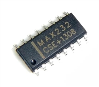 解读MAX232数据手册:全面剖析与应用推荐

 ATMEGA128数据手册解读:电气参数、引脚图
 温度传感器的常见故障及处理方法
 如何用万用表的欧姆档来辨别二极管的阴阳极
工作时间:9:00-21:00
CEO邮箱:ceo@jiepei.com
投诉邮箱:tousu@jiepei.com


 浙公网安备 33010502006866号 浙ICP备10014259号-119
营业执照ICP证
浙公网安备 33010502006866号 浙ICP备10014259号-119
营业执照ICP证


