AD570
FULL-SCALE CALIBRATION
The 5 kΩ thin-film input resistor is laser trimmed to produce a
current which matches the full-scale current of the internal
DAC—plus about 0.3%—when a full-scale analog input voltage
of 9.961 volts (10 volts—1 LSB) is applied at the input. The in-
put resistor is trimmed in this way so that if a fine trimming
potentiometer is inserted in series with the input signal, the in-
put current at the full-scale input voltage can be trimmed down
to match the DAC full-scale current as precisely as desired.
However, for many applications the nominal 9.961 volt full
scale can be achieved to sufficient accuracy by simply inserting a
15 Ω resistor in series with the analog input to Pin 13. Typical
full-scale calibration error will then be about ±2 LSB or ±0.8%.
If a more precise calibration is desired, a 200 Ω trimmer should
be used instead. Set the analog input at 9.961 volts, and set the
trimmer so that the output code is just at the transition between
11111110 and 11111111. Each LSB will then have a weight of
39.06 mV. If a nominal full scale of 10.24 volts is desired
(which makes the LSB have a value of exactly 40.00 mV), a
50 Ω resistor in series with a 200 Ω trimmer (or a 500 Ω trim-
mer with good resolution) should be used. Of course, larger full-
scale ranges can be arranged by using a larger input resistor, but
linearity and full-scale temperature coefficient may be compro-
mised if the external resistor becomes a sizable percentage of
5 kΩ.
Figure 5. Bipolar Offset Controlled by Logic Gate
Gate Output = 1: Unipolar 0 V–10 V Input Range
Gate Output = 0: Bipolar ±5 V Input Range
COMMON-MODE RANGE
The AD570 provides separate analog and digital common con-
nections. The circuit will operate properly with as much as
±200 mV of common-mode range between the two commons.
This permits more flexible control of system common bussing
and digital and analog returns.
BIPOLAR OPERATION
In normal operation the analog common terminal may generate
transient currents of up to 2 mA during a conversion. In addi-
tion, a static current of about 2 mA will flow into analog com-
mon in the unipolar mode after a conversion is complete. An
additional 1 mA will flow in during a blank interval with zero
analog input. The analog common current will be modulated by
the variations in input signal.
The standard unipolar 0 V to +10 V range is obtained by short-
ing the bipolar offset control pin to digital common. If the pin is
left open, the bipolar offset current will be switched into the
comparator summing node, giving a –5 V to +5 V range with an
The absolute maximum differential voltage rating between the
two commons is ±1 volt. We recommend that a parallel pair of
back-to-back protection diodes can be connected as shown in
Figure 6 if they are not connected locally.
Figure 4. Standard AD570 Connections
offset binary output code. (–5.00 volts in will give a 8-bit code
of 00000000; an input of 0.00 volts results in an output code of
10000000 and 4.96 volts at the input yields the 11111111 code.)
The bipolar offset control input is not directly TTL compatible,
but a TTL interface for logic control can be constructed as
shown in Figure 5.
Figure 6. Differential Common Voltage Protection
–4–
REV. A


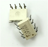
 TLP250光耦合器:资料手册参数分析

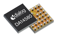
 DA14580 低功耗蓝牙系统级芯片(SoC):资料手册参数分析

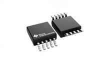
 INA226 高精度电流和功率监控器:资料手册参数分析

 SI2302 N沟道MOSFET:资料手册参数分析
