
 5秒后页面跳转

| 是否Rohs认证: | 不符合 | 生命周期: | Obsolete |
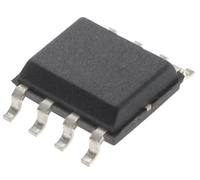
| 零件包装代码: | SOIC | 包装说明: | MS-012AA, SOIC-8 |
| 针数: | 8 | Reach Compliance Code: | not_compliant |
| ECCN代码: | EAR99 | HTS代码: | 8542.39.00.01 |
| 风险等级: | 5.21 | Is Samacsys: | N |
| 最大模拟输出电压: | 4.5 V | 最小模拟输出电压: | |
| 转换器类型: | D/A CONVERTER | 输入位码: | BINARY |
| 输入格式: | SERIAL | JESD-30 代码: | R-PDSO-G8 |
| JESD-609代码: | e0 | 长度: | 4.9 mm |
| 最大线性误差 (EL): | 0.0015% | 湿度敏感等级: | 1 |
| 位数: | 16 | 功能数量: | 1 |
| 端子数量: | 8 | 最高工作温度: | 70 °C |
| 最低工作温度: | 封装主体材料: | PLASTIC/EPOXY | |
| 封装代码: | SOP | 封装等效代码: | SOP8,.25 |
| 封装形状: | RECTANGULAR | 封装形式: | SMALL OUTLINE |
| 峰值回流温度(摄氏度): | 220 | 电源: | 5 V |
| 认证状态: | Not Qualified | 座面最大高度: | 1.75 mm |
| 标称安定时间 (tstl): | 1 µs | 子类别: | Other Converters |
| 最大压摆率: | 1.1 mA | 标称供电电压: | 3 V |
| 表面贴装: | YES | 技术: | CMOS |
| 温度等级: | COMMERCIAL | 端子面层: | Tin/Lead (Sn85Pb15) |
| 端子形式: | GULL WING | 端子节距: | 1.27 mm |
| 端子位置: | DUAL | 处于峰值回流温度下的最长时间: | 30 |
| 宽度: | 3.9 mm | Base Number Matches: | 1 |
| 型号 | 品牌 | 替代类型 | 描述 | 数据表 |
| AD5541CRZ | ADI |
完全替代  |
2.7 V to 5.5 V, Serial-Input, Voltage-Output, 16-Bit DACs |

|
| AD5541LRZ | ADI |
完全替代 |
2.7 V to 5.5 V, Serial-Input, Voltage-Output, 16-Bit DACs |
|
| AD5541CR | ADI |
完全替代 |
5 V, Serial-Input Voltage-Output, 16-Bit DACs |
|
| 型号 | 品牌 | 获取价格 | 描述 | 数据表 |
| AD5541LRZ | ADI |
获取价格 |
2.7 V to 5.5 V, Serial-Input, Voltage-Output, 16-Bit DACs |
|
| AD5541LRZ-REEL7 | ADI |
获取价格 |
2.7 V to 5.5 V, Serial-Input, Voltage-Output, 16-Bit DACs |
|
| AD5542 | ADI |
获取价格 |
5 V, Serial-Input Voltage-Output, 16-Bit DACs |
|
| AD5542_15 | ADI |
获取价格 |
2.7 V to 5.5 V, Serial-Input, Voltage-Output, 16-Bit DACs |
|
| AD5542A | ADI |
获取价格 |
2.7 V to 5.5 V, Serial-Input, Voltage-Output, 16-/12-Bit nanoDACs in LFCSP |
|
| AD5542AACPZ | ADI |
获取价格 |
2.7 V to 5.5 V, Serial-Input, Voltage-Output, 16-/12-Bit nanoDACs in LFCSP |
|
| AD5542AACPZ-REEL7 | ADI |
获取价格 |
Serial-Input Voltage-Output, 12-/16-Bit DAC |
|
| AD5542AARUZ | ADI |
获取价格 |
2.7 V to 5.5 V, Serial-Input, Voltage-Output, 16-/12-Bit nanoDACs in LFCSP |
|
| AD5542AARUZ-REEL7 | ADI |
获取价格 |
2.7 V to 5.5 V, Serial-Input, Voltage-Output, 16-Bit nano DAC™ in 10-lead LFCSP, |
|
| AD5542ABCPZ | ADI |
获取价格 |
2.7 V to 5.5 V, Serial-Input, Voltage-Output, 16-/12-Bit nanoDACs in LFCSP |
|
 解读BAV99LT1数据手册:产品特性、电气参数及替换型号推荐

 资料解析:P82B96TD引脚图说明、电气参数
 ATA6621N数据手册解读:产品特性、引脚图信息、电气参数
 一文AO3400引脚图、参数、产品特性
工作时间:9:00-21:00
CEO邮箱:ceo@jiepei.com
投诉邮箱:tousu@jiepei.com


 浙公网安备 33010502006866号 浙ICP备10014259号-119
营业执照ICP证
浙公网安备 33010502006866号 浙ICP备10014259号-119
营业执照ICP证


