(VDD = 3 V ؎ 10% or 5 V ؎ 10%, VSS = 0 V, VA = +VDD, VB = 0 V, –40؇C < TA < +85؇C,
AD5222–SPECIFICATIONS unless otherwise noted.)
Parameter
Symbol
Condition
Min
Typ1 Max
Unit
DC CHARACTERISTICS RHEOSTAT MODE (Specifications Apply to All VRs)
Resistor Differential NL2
R-DNL
R-INL
∆R
RWB, VA = NC
RWB, VA = NC
VAB = VDD, Wiper = No Connect, TA = 25°C –30
VAB = VDD, Wiper = No Connect
IW = VDD /R, VDD = 3 V or 5 V
CH 1 to 2, VAB = VDD, TA = 25°C
–1
–1
±1/4 +1
±0.4 +1
+30
LSB
LSB
%
ppm/°C
Ω
Resistor Nonlinearity2
Nominal Resistor Tolerance
Resistance Temperature Coefficient
Wiper Resistance3
RAB/∆T
–35
RW
∆R/RO
45
100
1
Nominal Resistance Match
0.2
%
DC CHARACTERISTICS POTENTIOMETER DIVIDER MODE (Specifications Apply to All VRs)
Resolution
N
7
Bits
Integral Nonlinearity4
INL
INL
DNL
RAB = 10 kΩ, 50 kΩ, or 100 kΩ
AB = 1 MΩ
–1
–2
–1
±1/4 +1
±1/2 +2
±1/4 +1
20
LSB
LSB
LSB
ppm/°C
LSB
LSB
R
Differential Nonlinearity4
Voltage Divider Temperature Coefficient ∆VW/∆T
Code = 40H
Code = 7FH
Code = 00H
Full-Scale Error
Zero-Scale Error
VWFSE
VWZSE
–1
0
–0.5 +0
0.5
1
RESISTOR TERMINALS
Voltage Range5
VA, B, W
CA, B
CW
VSS
VDD
V
Capacitance6 A, B
f = 1 MHz, Measured to GND, Code = 40H
f = 1 MHz, Measured to GND, Code = 40H
VA = VB = VW
45
60
1
pF
pF
nA
Capacitance6 W
Common-Mode Leakage
ICM
DIGITAL INPUTS AND OUTPUTS
Input Logic High
Input Logic Low
VIH
VIL
IIL
VDD = 5 V/3 V
VDD = 5 V/3 V
VIN = 0 V or 5 V
2.4/2.1
V
V
µA
pF
0.8/0.6
±1
Input Current
Input Capacitance6
CIL
5
POWER SUPPLIES
Power Single-Supply Range
Power Dual-Supply Range
Positive Supply Current
Negative Supply Current
Power Dissipation7
VDD RANGE
VDD/SS RANGE
IDD
ISS
PDISS
VSS = 0 V
2.7
±2.3
5.5
±2.7
40
V
V
µA
µA
µW
%/%
VIH = 5 V or VIL = 0 V
VSS = –2.5 V, VDD = +2.7 V
VIH = 5 V or VIL = 0 V, VDD = 5 V
15
15
40
150 400
0.002 0.05
Power Supply Sensitivity
PSS
DYNAMIC CHARACTERISTICS6, 8, 9
Bandwidth –3 dB
BW_10K
BW_50K
BW_100K
BW_1M
THDW
tS
RAB = 10 kΩ, Code = 40H
1000
180
78
kHz
kHz
kHz
kHz
%
µs
nV√Hz
R
R
R
AB = 50 kΩ, Code = 40H
AB = 100 kΩ, Code = 40H
AB = 500 kΩ, Code = 40H
VA = 1 V rms + 2 V dc, VB = 2 V dc, f = 1 kHz
RAB = 10 kΩ, ± 1 LSB Error Band
RWB = 5 kΩ, f = 1 kHz
7
Total Harmonic Distortion
VW Settling Time
Resistor Noise Voltage
0.005
2
14
eN_WB
INTERFACE TIMING CHARACTERISTICS (Applies to All Parts)6, 10
Input Clock Pulsewidth
CS to CLK Setup Time
tCH, tCL
tCSS
tCSH
tUDS
tUDH
tDSS
tDSH
tMDS
tMDH
Clock Level High or Low
30
20
20
10
30
20
30
20
40
ns
ns
ns
ns
ns
ns
ns
ns
ns
CS Rise to CLK Hold Time
U/D to Clock Fall Setup Time
U/D to Clock Fall Hold Time
DACSEL to Clock Fall Setup Time
DACSEL to Clock Fall Hold Time
MODE to Clock Fall Setup Time
MODE to Clock Fall Hold Time
NOTES
1Typicals represent average readings at 25°C, VDD = 5 V.
2Resistor position nonlinearity error R-INL is the deviation from an ideal value measured between the maximum resistance and the minimum resistance wiper positions.
R-DNL measures the relative step change from ideal between successive tap positions. Parts are guaranteed monotonic. See Figure 22 test circuit.
3Wiper resistance is not measured on the RAB = 1 MΩ models.
4INL and DNL are measured at VW with the RDAC configured as a potentiometer divider similar to a voltage output D/A converter. V A = VDD and VB = 0 V. DNL
specification limits of ±1 LSB maximum are guaranteed monotonic operating conditions. See Figure 21 test circuit.
5Resistor Terminals A, B, W have no limitations on polarity with respect to each other.
6Guaranteed by design and not subject to production test.
7PDISS is calculated from (IDD × VDD). CMOS logic level inputs result in minimum power dissipation.
8Bandwidth, noise and settling time are dependent on the terminal resistance value chosen. The lowest R value results in the fastest settling time and highest bandwidth.
The highest R value results in the minimum overall power consumption.
9All dynamic characteristics use VDD = 5 V.
10See timing diagram for location of measured values. All input control voltages are specified with tR = tF = 2.5 ns (10% to 90% of +3 V) and timed from a voltage level
of 1.5 V. Switching characteristics are measured using both VDD = 5 V or VDD = 3 V.
Specifications subject to change without notice.
REV. 0
–2–


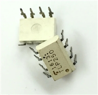
 TLP250光耦合器:资料手册参数分析

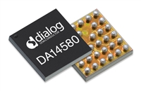
 DA14580 低功耗蓝牙系统级芯片(SoC):资料手册参数分析

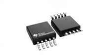
 INA226 高精度电流和功率监控器:资料手册参数分析

 SI2302 N沟道MOSFET:资料手册参数分析
