AD1892
(continued from Page 1)
DEFINITIONS
Dynamic Range
PRODUCT OVERVIEW (Continued)
The ratio of a full-scale input signal to the integrated noise in the
passband (0 kHz to ≈20 kHz), expressed in decibels (dB).
Dynamic range is measured with a –60 dB input signal and
“60 dB” arithmetically added to the result. This measurement
technique is consistent with the recommendations of the Audio
Engineering Society (AES17-1991) and the Electronic Industries
Association of Japan (EIAJ CP-307).
In addition to the Q-channel subcode and Channel Status buff-
ers, the AD1892 includes two 8-bit control registers and two 8-
bit status registers. The output data interface may be configured
in left-justified, I2S-justified and right-justified modes. The
AD1892 includes hardware power-down/reset and mute control
inputs, and power-down/reset and mute may also be invoked
through write to bits in the control registers. The AD1892
operates from a master clock that must be synchronous with the
output sample rate at 512 × FS. Cyclic Redundancy Coding
(CRC) error detection is performed over the full 80 bits of the
received Q-channel subcode information in consumer mode, as
well as the full 192 bits of the received Channel Status informa-
tion in professional mode.
Total Harmonic Distortion + Noise
Total Harmonic Distortion plus Noise (THD+N) is defined as
the ratio of the square root of the sum of the squares of the
values of the harmonics and noise to the value of the fundamen-
tal input frequency. It is usually expressed in percent (%) or
decibels.
Interchannel Phase Deviation
Difference in input sampling times between stereo channels,
expressed as a phase difference in degrees between 1 kHz inputs.
The AD1892 includes a SYNC input (Pin 23) that allows
multiple AD1892s in a system to be synchronized to a common
LEFT/RIGHT clock.
Group Delay
The AD1892 is offered in a 28-lead SOIC package. It operates
over the industrial temperature range from –40°C to +85°C
at a supply voltage from 4.5 V to 5.5 V. The only external
components required to support the AD1892 are power supply
decoupling capacitors.
The time interval required for the frequency components of an
input pulse to appear at the converter’s output, expressed in
milliseconds (ms). More precisely, the derivative of radian phase
with respect to radian frequency at a given frequency.
AD1892 PIN LIST
Biphase-Mark Serial Input
Pin Name SOIC
I/O
Description
RXP
RXN
13
14
I
I
Positive differential biphase-mark serial digital audio receiver input. 20 mV hysteresis.
Negative differential biphase-mark serial digital audio receiver input. 20 mV hysteresis.
Serial Output Interface
Pin Name SOIC I/O
Description
SDATA
24
O
Serial output, MSB first, containing two channels of 16 to 20 bits (default) of twos-complement
data per channel, depending on control register settings. The data can be configured in I2S-justified
(default), left-justified, and right-justified orientations, depending on control register settings. See
Figure 36 for timing.
BCLK
LRCLK
SYNC
26
25
23
O
O
I
Bit clock output for output data. Frequency is either 32 × FS (packed mode) or 64 × FS (default),
depending on control register settings. See Figure 36 for timing.
LEFT/RIGHT clock output for output data. Runs continuously and is a synchronous divide-down
from MCLK (MCLK/512). See Figure 36 for timing.
The SYNC input allows multiple AD1892s in a system to be phase and group delay synchronized to
the same LEFT/RIGHT clock. The SYNC signal resets internal AD1892 counters such that 512 MCLK
cycles after the falling edge of SYNC, the AD1892 data will be valid, and the AD1892 LRCLK signal
will change state. It is recommended that the SYNC input be used only when the AD1892 is in the
64 × FSOUT BCLK mode (default configuration). GND when not in use.
Decoded Channel Status Outputs
Pin Name SOIC
I/O
Description
CA
21
O
In consumer or professional mode, CA is the inverse of Channel Status Bit 1, Byte 0 (C1, audio/
nonaudio). CA = 0 indicates nonaudio, CA = 1 indicates audio. CA = 0 can be used to indicate
Dolby AC-3 encoded data.
CB
20
O
In consumer mode, CB is the inverse of Channel Status Bit 2, Byte 0 (C2, copy/copyright). CB = 0
indicates copy permitted/copyright not asserted; CB = 1 indicates copy inhibited/copyright asserted.
In professional mode, CB is defined as EM0, the least significant bit of the two bits that encodes the
emphasis status of the audio material.
REV. 0
–4–


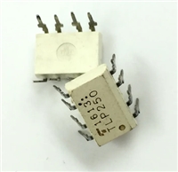
 TLP250光耦合器:资料手册参数分析

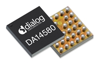
 DA14580 低功耗蓝牙系统级芯片(SoC):资料手册参数分析

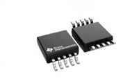
 INA226 高精度电流和功率监控器:资料手册参数分析

 SI2302 N沟道MOSFET:资料手册参数分析
