AD1877
PIN FUNCTION DESCRIPTIONS
Pin
Signal to Total Harmonic Distortion (S/THD)
The ratio of the rms value of the fundamental input signal to the
rms sum of all harmonically related spectral components in the
passband, expressed in decibels.
Input/
Pin
Output Name
Description
1
2
3
4
5
6
7
8
I/O
I/O
I/O
I
I
I
I
I
I
I
O
O
I
O
O
I
O
O
I
I
I
I
I
LRCK
WCLK
BCLK
DVDD1
DGND1
Left/Right Clock
Word Clock
Bit Clock
5 V Digital Supply
Digital Ground
Passband
The region of the frequency spectrum unaffected by the attenu-
ation of the digital decimator’s filter.
Passband Ripple
The peak-to-peak variation in amplitude response from equal-
amplitude input signal frequencies within the passband,
expressed in decibels.
RDEDGE Read Edge Polarity Select
S/M
384/256
AVDD
VINL
CAPL1
CAPL2
AGNDL
Slave/Master Select
Clock Mode
5 V Analog Supply
Left Channel Input
Left External Filter Capacitor 1
Left External Filter Capacitor 2
Left Analog Ground
Left Reference Voltage Output
Right Reference Voltage Output
Right Analog Ground
Stopband
The region of the frequency spectrum attenuated by the digital
decimator’s filter to the degree specified by “stopband
attenuation.”
9
10
11
12
13
14
15
16
17
18
19
20
21
22
23
24
25
26
27
28
Gain Error
With a near full-scale input, the ratio of actual output to
expected output, expressed as a percentage.
V
REFL
Interchannel Gain Mismatch
With identical near full-scale inputs, the ratio of outputs of the
two stereo channels, expressed in decibels.
VREF
R
AGNDR
CAPR2
CAPR1
VINR
AGND
RLJUST
Right External Filter Capacitor 2
Gain Drift
ght External Filter
Change in response to a near full-scale input with a change in
temperature, expressed as parts-per-million (ppm) per °C.
Ri
Capacitor 1
Right Channel Input
Analog Ground
Right/Left Justify
Midscale Offset Error
Output response to a midscale dc input, expressed in least-
significant bits (LSBs).
MSBDLY Delay MSB One BCLK Period
Midscale Drift
RESET
DGND2
DVDD2
SOUT
TAG
Reset
Change in midscale offset error with a change in temperature,
expressed as parts-per-million (ppm) per °C.
I
I
O
O
I
Digital Ground
5 V Digital Supply
Serial Data Output
Serial Overrange Output
Master Clock
Crosstalk (EIAJ Method)
Ratio of response on one channel with a grounded input to a
full-scale 1 kHz sine-wave input on the other channel, expressed
in decibels.
CLKIN
Power Supply Rejection
DEFINITIONS
Dynamic Range
With no analog input, signal present at the output when a
300 mV p-p signal is applied to power supply pins, expressed in
decibels of full scale.
The ratio of a full-scale output signal to the integrated output
noise in the passband (20 Hz to 20 kHz), expressed in decibels
(dB). Dynamic range is measured with a –60 dB input signal
and is equal to (S/[THD+N]) 60 dB. Note that spurious har-
monics are below the noise with a –60 dB input, so the noise
level establishes the dynamic range. The dynamic range is speci-
fied with and without an A-Weight filter applied.
Group Delay
Intuitively, the time interval required for an input pulse to
appear at the converter’s output, expressed in milliseconds
(ms). More precisely, the derivative of radian phase with respect
to radian frequency at a given frequency.
Group Delay Variation
Signal to (Total Harmonic Distortion + Noise)
(S/(THD + N))
The ratio of the root-mean-square (rms) value of the fundamen-
tal input signal to the rms sum of all other spectral components
in the passband, expressed in decibels (dB).
The difference in group delays at different input frequencies.
Specified as the difference between largest and the smallest
group delays in the passband, expressed in microseconds (µs).
–5–
REV. A


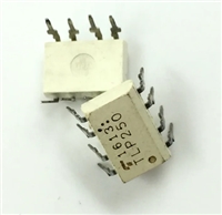
 TLP250光耦合器:资料手册参数分析

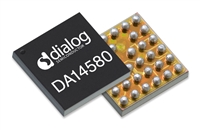
 DA14580 低功耗蓝牙系统级芯片(SoC):资料手册参数分析

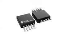
 INA226 高精度电流和功率监控器:资料手册参数分析

 SI2302 N沟道MOSFET:资料手册参数分析
