A49LF040
*Comments
ABSOLUTE MAXIMUM RATINGS*
Stresses above those listed under "Absolute Maximum Ratings" may
cause permanent damage to this device. These are stress ratings
only. Functional operation of this device at these or any other
conditions above those indicated in the operational sections of these
specifications are not implied or intended. Exposure to the absolute
maximum rating conditions for extended periods may affect device
reliability.
Temperature Under Bias . . . . . . . . . .. . . . -55°C to + 125°C
Storage Temperature . . . . . . . . . . . . . . . . . -65°C to + 125°C
D.C. Voltage on Any Pins with Respect to Ground (1)
. . . . . . . . . . . . . . . . . . . . . . . . . ... . . . . . -0.5V to VDD + 0.5V
Package Power Dissipation Capability (Ta=25°C)
. . . . . . . . . . . . . . . . . . . . . . . . …. . . . . . -0.5V to VDD + 0.5V
Output Short Circuit Current (2) . . . . . . . . . .. . . . . . . 50mA
Operating Ranges
Notes:
Commercial (C) Devices
1. Minimum DC voltage on input or I/O pins is -0.5V. During voltage
transitions, input or I/O pins may undershoot VSS to -2.0V for
periods of up to 20ns. Maximum DC voltage on input and I/O
pins is VDD + 0.5V. During voltage transitions, input or I/O pins
may overshoot to VDD + 2.0V for periods up to 20ns.
Ambient Temperature (TA) . . . . . . . . ….. . . . . . 0°C to +85°C
VDD Supply Voltages
VDD for all devices . . . . . . . . . . . . . . . . ….. . +3.0V to +3.6V
Operating ranges define those limits between which the
functionally of the device is guaranteed.
2. No more than one output is shorted at a time. Duration of the
short circuit should not be greater than one second.
MODE SELECTION
LPC Read Operation
LPC Read operations read from the memory cells or specific
registers in the LPC device. A valid LPC Read operation
starts when LFRAME# is Low as LCLK rises and a START
value “0000b” is on LAD[3:0] then the next nibble “010X” is
on LAD[3:0]. Addresses and data are transferred to and from
the device decided by a series of “fields”. Field sequences
and contents are strictly defined for LPC Read operations.
Refer to Table 2 for LPC Read Cycle Definition.
The A49LF040 flash memory devices can operate in two
distinct interface modes: the Low Pin Count Interface
(LPC) mode and the Address/Address Multiplexed (A/A Mux)
mode. The Mode pin is used to set the interface mode
selection. If the Mode pin is set to logic High, the device is in
A/A Mux mode; while if the Mode pin is set Low, the device is
in the LPC mode. The Mode pin must be configured prior to
device operation. The Mode pin is internally pulled down if
the pin is not connected. In LPC mode, the device is
configured to interface with its host using Intel’s Low Pin
Count proprietary protocol. Communication between Host
and the A49LF040 occurs via the 4-bit I/O communication
signals, LAD[3:0] and the LFRAME#. In A/A Mux mode, the
device is programmed via an 11-bit address A10-A0 and an 8-
bit data I/O7-I/O0 parallel signals. The address inputs are
multiplexed in row and column selected by control signal
R/C# pin. The column addresses are mapped to the higher
internal addresses, and the row addresses are mapped to
the lower internal addresses. See the Device Memory Maps
in Figure 3 for address assignment.
LPC Write Operation
LPC Write operations write to the LPC Interface or LPC
registers. A valid LPC Write operation starts when LFRAME#
is Low as LCLK rises and a START value “0000b” is on
LAD[3:0] then the next nibble “011X” is on LAD[3:0].
Addresses and data are transferred to and from the device
decided by a series of “fields”. Field sequences and contents
are strictly defined for LPC Write operations. Refer to Table 3
for LPC write Cycle Definition.
LPC Abort Operation
If LFRAME# is driven low for one or more clock cycles during
a LPC cycle, the cycle will be terminated and the device will
wait for the ABORT command. The host may drive the
LAD[3:0] with ‘1111b’ (ABORT command) to return the
device to Ready mode. If abort occurs during a Write
operation such as checking the operation status with Data#
Polling (I/O7) or Toggle Bit (I/O6) pins, the read status cycle
will be aborted but the internal write operation will not be
affected. In this case, only the reset operation initiated by
RST# or INIT# pin can terminate the Write operation..
LPC MODE OPERATION
The LPC interface consists of four data signals (LAD[3:0]),
one control signal (LFRAME#) and a clock (LCLK). The data
signals, control signal and clock comply with PCI
specifications. Operations such as Memory Read and
Memory Write use Intel LPC propriety protocol. JEDEC
Standard SDP (Software Data Protection) Byte-Program and
Block-Erase command sequences are incorporated into the
LPC memory cycles. Chip-Erase command is only available
in A/A Mux mode. The addresses and data are transferred
through LAD[3:0] synchronized with the input clock LCLK
during a LPC memory cycle. The pulse of LFRAME# is
inserted for at least one clock period to indicate the start of a
LPC memory cycle. The address or data on LAD[3:0] is
latched on the rising edge of LCLK. The device enters
standby mode when LFRAME# is high and no internal
operation is in progress. The device is in ready mode when
LFRAME# is low and no activity is on the LPC bus.
Response To Invalid Fields
During LPC operations, the LPC will not explicitly indicate
that it has received invalid field sequences. The response to
specific invalid fields or sequences is as follows:
Address out of range: The A49LF040 will only response to
address range as specified in Table 4. Address A22 has the
special function of directing reads and writes to the flash
memory (A22=1) or to the register space (A22=0).
PRELIMINARY
(August, 2004, Version 0.1)
5
AMIC Technology, Corp.


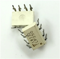
 TLP250光耦合器:资料手册参数分析

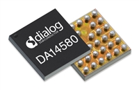
 DA14580 低功耗蓝牙系统级芯片(SoC):资料手册参数分析

 INA226 高精度电流和功率监控器:资料手册参数分析

 SI2302 N沟道MOSFET:资料手册参数分析
