A3958
DMOS Full-Bridge PWM Motor Driver
FUNCTIONAL DESCRIPTION (continued)
D15 Phase Logic. Bit D15, in conjunction with PHASE,
determines if the device is operating in the forward
(PHASE ≠ D15) or reverse (PHASE = D15) state.
D18 Test Mode. Bit D18 low (default) operates the
device in normal mode. D18 is only used for testing
purposes. The user should never change this bit.
PHASE D15 State
OUTA OUTB
D19 Sleep Mode. Bit D19 selects a Sleep mode to
minimize power consumption when not in use. This
disables much of the internal circuitry including the
regulator and charge pump. On power up the serial port is
initialized to all 0s. Bit D19 should be programmed high
for 1 ms before attempting to enable any output driver.
0
1
0
1
0
0
1
1
Reverse
Forward
Forward
Reverse
Low
High
High
Low
High
Low
Low
High
D16 Gm Range Select. Bit D16, in conjunction with
RANGE, determines if VREF is divided by 5 (RANGE ≠
D16) or by 10 (RANGE = D16).
D19
Sleep Mode
0
1
Sleep
Normal
RANGE
D16
Divider
Serial Port Write Timing Operation. Data is clocked
into the shift register on the rising edge of the CLOCK
signal. Normally STROBE will be held high, only brought
low to initiate a write cycle. Refer to diagram below and
these specifications for the minimum timing requirements.
A. DATA setup time ........................................... 15 ns
B. DATA hold time ............................................ 10 ns
C. Setup STROBE to CLOCK rising edge ........ 50 ns
D. CLOCK high pulse width ............................. 50 ns
E. CLOCK low pulse width ............................... 50 ns
F. Setup CLOCK rising edge to STROBE ........ 50 ns
G. STROBE pulse width ................................... 50 ns
0
1
0
1
0
0
1
1
÷10
÷5
÷5
÷10
D17 Internal PWM Mode. Bit D17, in conjunction with
MODE, selects slow (MODE ≠ D17) or mixed (MODE =
D17) current decay.
MODE D17 Current-Decay Mode
0
1
0
1
0
0
1
1
Mixed
Slow
Slow
Mixed
VREG. This internally generated voltage is used to operate
the sink-side DMOS outputs. The VREG terminal should
be decoupled with a 0.22 μF capacitor to ground. VREG is
Serial Port Write Timing
STROBE
CLOCK
E
C
D
F
G
A
B
D19
D18
D0
DATA
Dwg. WP-038
Allegro MicroSystems, Inc.
115 Northeast Cutoff
6
Worcester, Massachusetts 01615-0036 U.S.A.
1.508.853.5000; www.allegromicro.com


 MAX6675资料手册参数详解、引脚配置说明

 LM258引脚图及功能介绍、主要参数分析

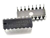
 CD4052资料手册参数详解、引脚配置说明

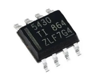
 一文带你了解TPS5430资料手册分析:参数介绍、引脚配置说明
