A25L40P Series
SIGNAL DESCRIPTION
(
) Low enables the device, placing it in the active power
S
mode.
Serial Data Output (Q). This output signal is used to transfer
data serially out of the device. Data is shifted out on the
falling edge of Serial Clock (C).
After Power-up, a falling edge on Chip Select ( ) is required
S
prior to the start of any instruction.
Serial Data Input (D). This input signal is used to transfer
data serially into the device. It receives instructions,
addresses, and the data to be programmed. Values are
latched on the rising edge of Serial Clock (C).
Serial Clock (C). This input signal provides the timing of the
serial interface. Instructions, addresses, or data present at
Serial Data Input (D) are latched on the rising edge of Serial
Clock (C). Data on Serial Data Output (Q) changes after the
falling edge of Serial Clock (C).
Hold (
). The Hold (
) signal is used to pause
HOLD
HOLD
any serial communications with the device without
deselecting the device.
During the Hold condition, the Serial Data Output (Q) is high
impedance, and Serial Data Input (D) and Serial Clock (C)
are Don’t Care. To start the Hold condition, the device must
be selected, with Chip Select ( ) driven Low.
S
Write Protect ( ). The main purpose of this input signal is
W
Chip Select ( ). When this input signal is High, the device is
S
to freeze the size of the area of memory that is protected
against program or erase instructions (as specified by the
values in the BP2, BP1 and BP0 bits of the Status Register).
deselected and Serial Data Output (Q) is at high impedance.
Unless an internal Program, Erase or Write Status Register
cycle is in progress, the device will be in the Standby mode
(this is not the Deep Power-down mode). Driving Chip Select
SPI MODES
falling edge of Serial Clock (C).
These devices can be driven by a microcontroller with its SPI
peripheral running in either of the two following modes:
– CPOL=0, CPHA=0
– CPOL=1, CPHA=1
For these two modes, input data is latched in on the rising
edge of Serial Clock (C), and output data is available from the
The difference between the two modes, as shown in Figure 2,
is the clock polarity when the bus master is in Stand-by mode
and not transferring data:
– C remains at 0 for (CPOL=0, CPHA=0)
– C remains at 1 for (CPOL=1, CPHA=1)
PRELIMINARY (May, 2007, Version 0.4)
3
AMIC Technology Corp.


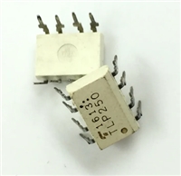
 TLP250光耦合器:资料手册参数分析

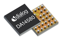
 DA14580 低功耗蓝牙系统级芯片(SoC):资料手册参数分析

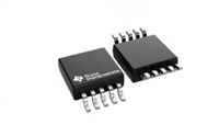
 INA226 高精度电流和功率监控器:资料手册参数分析

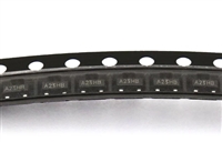
 SI2302 N沟道MOSFET:资料手册参数分析
