932SQ426
CK420BQ DERIVATIVE SUPPORTING SRNS PCIE CLOCKING
Pin Descriptions (TSSOP)
PIN #
PIN NAME
SMBCLK
TYPE
IN Clock pin of SMBUS circuitry, 5V tolerant
DESCRIPTION
1
2
3
4
GND14
AVDD14
VDD14
PWR Ground pin for 14MHz output and logic.
PWR Analog power pin for 14MHz PLL
PWR Power pin for 14MHz output and logic
14.318 MHz reference clock. 3X drive strength as default / TEST_SEL latched input to enable test mode.
Refer to Test Clarification Table. This pin has a weak (~120Kohm) internal pull down.
5
vREF14_3x/TEST_SEL I/O
6
7
8
GND14
GNDXTAL
X1_25
PWR Ground pin for 14MHz output and logic.
PWR Ground pin for Crystal Oscillator.
IN Crystal input, Nominally 25.00MHz.
9
X2_25
OUT Crystal output, Nominally 25.00MHz.
10
11
12
13
14
15
16
17
18
19
20
21
22
23
VDDXTAL
GNDPCI
VDDPCI
PCI4_2x
PCI3_2x
PCI2_2x
PCI1_2x
PCI0_2x
GNDPCI
VDDPCI
VDD48
PWR 3.3V power for the crystal oscillator.
PWR Ground pin for PCI outputs and logic.
PWR 3.3V power for the PCI outputs and logic
OUT 3.3V PCI clock output
OUT 3.3V PCI clock output
OUT 3.3V PCI clock output
OUT 3.3V PCI clock output
OUT 3.3V PCI clock output
PWR Ground pin for PCI outputs and logic.
PWR 3.3V power for the PCI outputs and logic
PWR 3.3V power for the 48MHz output and logic
OUT 3.3V 48MHz output
PWR Ground pin for 48MHz output and logic.
PWR Ground pin for DOT96 output and logic.
True clock of differential 96MHz output. These are current mode outputs and external series resistors
OUT and shunt resistors are required for termination. See Test Loads and Recommended Terminations for
specific values.
48M_2x
GND48
GND96
24
25
DOT96T
DOT96C
Complementary clock of differential 96MHz output. These are current mode outputs and external series
OUT resistors and shunt resistors are required for termination. See Test Loads and Recommended
Terminations for specific values.
26
27
AVDD96
PWR 3.3V power for the 48/96MHz PLL and the 96MHz output and logic
TEST_MODE is a real time input to select between Hi-Z and REF/N divider mode while in test mode.
TEST_MODE
IN
Refer to Test Clarification Table.
CKPWRGD# is an active low input used to sample latched inputs and allow the device to Power Up. PD is
IN an asynchronous active high input pin used to put the device into a low power state. The internal clocks
and PLLs are stopped.
28
29
30
CKPWRGD#/PD
VDDSRC
PWR 3.3V power for the SRC outputs and logic
True clock of differential SRC output. These are current mode outputs and external series resistors and
OUT shunt resistors are required for termination. See Test Loads and Recommended Terminations for specific
values.
SRC0T
Complementary clock of differential SRC output. These are current mode outputs and external series
OUT resistors and shunt resistors are required for termination. See Test Loads and Recommended
Terminations for specific values.
31
32
33
SRC0C
GNDSRC
SRC1C
PWR Ground pin for SRC outputs and logic.
Complementary clock of differential SRC output. These are current mode outputs and external series
OUT resistors and shunt resistors are required for termination. See Test Loads and Recommended
Terminations for specific values.
True clock of differential SRC output. These are current mode outputs and external series resistors and
OUT shunt resistors are required for termination. See Test Loads and Recommended Terminations for specific
values.
34
35
36
SRC1T
SRC2C
SRC2T
37
38
39
VDDSRC
AVDD_SRC
GNDSRC
PWR 3.3V power for the SRC outputs and logic
PWR 3.3V power for the SRC PLL analog circuits
PWR Ground pin for SRC outputs and logic.
This pin establishes the reference current for the differential current-mode output pairs. This pin requires a
OUT fixed precision resistor tied to ground in order to establish the appropriate current. 475 ohms is the
standard value.
40
IREF
IDT® CK420BQ DERIVATIVE SUPPORTING SRNS PCIE CLOCKING
3
932SQ426
REV C 022916


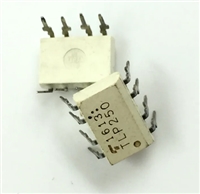
 TLP250光耦合器:资料手册参数分析

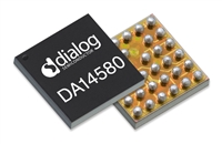
 DA14580 低功耗蓝牙系统级芯片(SoC):资料手册参数分析

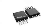
 INA226 高精度电流和功率监控器:资料手册参数分析

 SI2302 N沟道MOSFET:资料手册参数分析
