78P2351
Single Channel
OC-3/ STM1-E/ E4 LIU
Reference
Clock
Plesiochronous Tx Serial Mode
Figure 3 represents a common condition where a
serial transmit clock is not available and/or the data
is not source synchronous to the reference clock
CKREFP/N
PI[3:0]D
CMI
CMI
Coax
Coax
4-bit CMOS TTL
34/39 MHz
CMIP/N
RXP/N
XFMR
XFMR
PIxCK
provided to the 78P2351.
In this mode, the
Framer/
Mapper
TDK
78P2351 will recover a transmit clock from the serial
plesiochronous data and bypass the internal FIFO
and re-timing block. This mode is commonly used
for mezzanine cards, modules, and any application
where the reference clock can’t always be
synchronous to the transmit source clock/data.
78P2351
PO[3:0]D
POCK
4-bit CMOS TTL
34/39 MHz
Figure 4: Slave Parallel Mode
Reference
Clock
Reference
Clock
XO
CKREFP
CKREFP/N
NRZ
CMI
CMI
Coax
Coax
PI[3:0]D
PTOCK
CMI
CMI
Coax
4-bit CMOS TTL
34/39 MHz
CMIP/N
RXP/N
SIDP/N
XFMR
XFMR
CMIP/N
RXP/N
XFMR
Framer/
Mapper
TDK
NRZ
Framer/
Mapper
TDK
78P2351
SOCKP/N
SODP/N
140 / 155 MHz
78P2351
PO[3:0]D
POCK
4-bit CMOS TTL
34/39 MHz
Coax
XFMR
Figure 3: Plesiochronous data only
(Tx CDR enabled, FIFO bypassed)
Figure 5: Master Parallel Mode
Synchronous Parallel Modes
Transmit FIFO Description
In parallel modes, 4-bit CMOS data segments are
input to the chip with a 34.816MHz (E4 ÷ 4) or
38.88MHz (STM1 ÷ 4) synchronous clock. These
inputs are re-timed in a 4x8 clock decoupling FIFO
and then to a serializer for transmission. Because
the data is passed through the FIFO and re-timed
using a synthesized clock, the transmit nibble clock
and data must be source synchronous to the
provided reference clock.
Since the reference clock and transmit clock/data go
through different delay paths, it is inevitable that the
phase relationship between the two clocks can vary
in a bounded manner due to the fact that the
absolute delays in the two paths can vary over time.
The transmit FIFO allows long-term clock phase drift
between the Tx clock and system reference clock,
not exceeding +/- 25.6ns, to be handled without
transmit error. If the clock wander exceeds the
specified limits, the FIFO will over or under flow, and
the FERR register signal will be asserted. This
signal can be used to trigger an interrupt. This
interrupt event is automatically cleared when a FIFO
Reset (FRST) pulse is applied, and the FIFO is re-
centered.
For maximum compatibility with legacy ASICs, the
78P2351 can operate in both slave and master clock
modes as shown in Figures 4 and 5 respectively.
Note: A loop-timing mode is also available to
allow external remote loopbacks (i.e. line
loopback in framer). In this mode, the FIFO is
still enabled, but the transmit data will be re-
timed using the recovered receive clock.
Notes:
1) External remote loopbacks (i.e. loopback
within framer) are not possible in
synchronous operation (FIFO enabled)
unless the data is re-justified to be
synchronous to the system reference clock
or the 78P2351 is configured for loop-timing
operation.
2) During IC power-up or transmit power-up,
the clocks going to the FIFO may not be
stable and cause the FIFO to overflow or
underflow. As such, the FIFO should be
manually reset using FRST anytime the
transmitter is powered-up.
HW Control Pins SW Control Bits
SDI_PAR CKMODE
Parallel
Mode
PAR
PMODE
Slave
High
High
Low
1
0
Slave +
Float
1
1
0
1
*Loop-timing
Master
High
High
*To enable loop-timing in software mode, set
SMOD[1:0]=11
Page: 6 of 42
2006 Teridian Semiconductor Corporation
Rev. 2.4


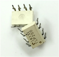
 TLP250光耦合器:资料手册参数分析

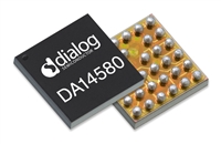
 DA14580 低功耗蓝牙系统级芯片(SoC):资料手册参数分析

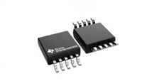
 INA226 高精度电流和功率监控器:资料手册参数分析

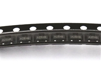
 SI2302 N沟道MOSFET:资料手册参数分析
