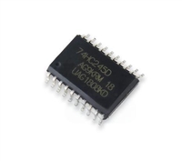
5秒后页面跳转
5962-8772101CA PDF预览

5962-8772101CA

更新时间: 2024-02-19 17:55:07
品牌 Logo 应用领域
德州仪器 - TI 总线驱动器总线收发器逻辑集成电路输出元件
页数 文件大小 规格书
17页 637K
描述
QUADRUPLE BUS BUFFER GATES WITH 3-STATE OUTPUTS

5962-8772101CA 技术参数

生命周期:Obsolete零件包装代码:DFP
包装说明:DFP,针数:14
Reach Compliance Code:unknownHTS代码:8542.39.00.01
风险等级:5.74系列:HC/UH
JESD-30 代码:R-GDFP-F14逻辑集成电路类型:BUS DRIVER
位数:1功能数量:4
端口数量:2端子数量:14
最高工作温度:125 °C最低工作温度:-55 °C
输出特性:3-STATE输出极性:TRUE
封装主体材料:CERAMIC, GLASS-SEALED封装代码:DFP
封装形状:RECTANGULAR封装形式:FLATPACK
传播延迟(tpd):150 ns认证状态:Not Qualified
筛选级别:MIL-STD-883最大供电电压 (Vsup):6 V
最小供电电压 (Vsup):2 V标称供电电压 (Vsup):4.5 V
表面贴装:YES技术:CMOS
温度等级:MILITARY端子形式:FLAT
端子位置:DUALBase Number Matches:1

5962-8772101CA 数据手册

 浏览型号5962-8772101CA的Datasheet PDF文件第1页浏览型号5962-8772101CA的Datasheet PDF文件第3页浏览型号5962-8772101CA的Datasheet PDF文件第4页浏览型号5962-8772101CA的Datasheet PDF文件第5页浏览型号5962-8772101CA的Datasheet PDF文件第6页浏览型号5962-8772101CA的Datasheet PDF文件第7页 
ꢀ ꢁꢂ ꢃꢄ ꢅ ꢆꢇ ꢂꢈ ꢀꢁ ꢉ ꢃ ꢄꢅꢆ ꢇ ꢂ  
ꢊꢋ ꢌ ꢍꢎ ꢋ ꢏꢐ ꢑ ꢒꢋ ꢀ ꢒꢋ ꢓꢓ ꢑꢎ ꢔ ꢌꢕꢑ ꢀ  
ꢖꢗ ꢕ ꢄ ꢘ ꢙꢀꢕꢌꢕ ꢑ ꢚꢋꢕ ꢏꢋ ꢕꢀ  
SCLS104D − MARCH 1984 − REVISED AUGUST 2003  
FUNCTION TABLE  
(each buffer)  
INPUTS  
OUTPUT  
Y
OE  
A
H
L
L
L
H
L
H
X
Z
logic diagram (positive logic)  
1
10  
1OE  
3OE  
3A  
2
3
6
9
8
1A  
1Y  
2Y  
3Y  
4Y  
4
13  
12  
2OE  
4OE  
4A  
5
11  
2A  
Pin numbers shown are for the D, DB, J, N, NS, PW, and W packages.  
absolute maximum ratings over operating free-air temperature range (unless otherwise noted)  
Supply voltage range, V  
. . . . . . . . . . . . . . . . . . . . . . . . . . . . . . . . . . . . . . . . . . . . . . . . . . . . . . . . . . −0.5 V to 7 V  
CC  
I
Input clamp current, I (V < 0 or V > V ) (see Note 1) . . . . . . . . . . . . . . . . . . . . . . . . . . . . . . . . . . . . 20 mA  
IK  
I
CC  
Output clamp current, I  
(V < 0 or V > V ) (see Note 1) . . . . . . . . . . . . . . . . . . . . . . . . . . . . . . . . 20 mA  
OK  
O O CC  
Continuous output current, I (V = 0 to V ) . . . . . . . . . . . . . . . . . . . . . . . . . . . . . . . . . . . . . . . . . . . . . . 35 mA  
Continuous current through V  
O
O
CC  
CC  
or GND . . . . . . . . . . . . . . . . . . . . . . . . . . . . . . . . . . . . . . . . . . . . . . . . . . . 70 mA  
Package thermal impedance, θ (see Note 2): D package . . . . . . . . . . . . . . . . . . . . . . . . . . . . . . . . . . . 86°C/W  
JA  
DB package . . . . . . . . . . . . . . . . . . . . . . . . . . . . . . . . . 96°C/W  
N package . . . . . . . . . . . . . . . . . . . . . . . . . . . . . . . . . . . 80°C/W  
NS package . . . . . . . . . . . . . . . . . . . . . . . . . . . . . . . . . 76°C/W  
PW package . . . . . . . . . . . . . . . . . . . . . . . . . . . . . . . . 113°C/W  
Storage temperature range, T  
. . . . . . . . . . . . . . . . . . . . . . . . . . . . . . . . . . . . . . . . . . . . . . . . . . . −65°C to 150°C  
stg  
Stresses beyond those listed under “absolute maximum ratings” may cause permanent damage to the device. These are stress ratings only, and  
functional operation of the device at these or any other conditions beyond those indicated under “recommended operating conditions” is not  
implied. Exposure to absolute-maximum-rated conditions for extended periods may affect device reliability.  
NOTES: 1. The input and output voltage ratings may be exceeded if the input and output current ratings are observed.  
2. The package thermal impedance is calculated in accordance with JESD 51-7.  
2
POST OFFICE BOX 655303 DALLAS, TEXAS 75265  

与5962-8772101CA相关器件

型号 品牌 描述 获取价格 数据表
5962-8772101CX ETC 4-Bit Buffer/Driver

获取价格

5962-8772101DX ETC 4-Bit Buffer/Driver

获取价格

5962-87722012A TI High Speed CMOS Logic Triple 3-Input OR Gate

获取价格

5962-87722012X ETC Triple 3-input OR Gate

获取价格

5962-8772201CA TI High Speed CMOS Logic Triple 3-Input OR Gate

获取价格

5962-8772201CX ETC Triple 3-input OR Gate

获取价格