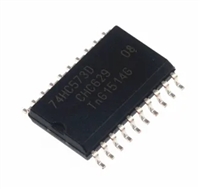
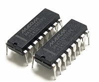
1.2.4 Case outline(s). The case outline(s) are as designated in MIL-STD-1835 and as follows:
Outline letter
Descriptive designator
Terminals
Package style
G
P
Z
MACY1-X8
GDIP1-T8 or CDIP2-T8
GDFP1-G14
8
8
14
Can
Dual-in-line
Flat pack with gullwing leads
1.2.5 Lead finish. The lead finish is as specified in MIL-PRF-38535 for device classes Q and V or MIL-PRF-38535,
appendix A for device class M.
1.3 Absolute maximum ratings. 1/
Supply voltage (±V ) ..................................................................... ±18 V
CC
Power dissipation (P ) ..................................................................... 500 mW 2/
D
Input voltage (V ) ............................................................................ ±18 V 3/
IN
Logic to logic differential voltage ...................................................... +7 V, -30 V 4/
Output short circuit duration ............................................................. Indefinite
Hold capacitor short circuit duration ................................................. 10 seconds
Lead temperature (soldering, 10 seconds) ...................................... 300°C
Storage temperature range .............................................................. -65°C to +150°C
Junction temperature (T ) ................................................................ +150°C
J
Thermal resistance, junction-to-case (θ ):
JC
Case G .......................................................................................... 48°C/W
Case P .......................................................................................... See MIL-STD-1835
Case Z .......................................................................................... 20°C/W
Thermal resistance, junction-to-ambient (θ ):
JA
Case G .......................................................................................... 160°C/W, still air at 0.5 W
84°C/W, 500 LFPM air flow 0.5 W
Case P .......................................................................................... 120°C/W
Case Z .......................................................................................... 140°C/W, still air at 0.5 W
95°C/W, 500 LFPM air flow 0.5 W
1.4 Recommended operating conditions.
Supply voltage (±V ) ..................................................................... ±15 V
CC
Ambient operating temperature range (T ) ...................................... -55°C to +125°C
A
2. APPLICABLE DOCUMENTS
2.1 Government specification, standards, and handbooks. The following specification, standards, and handbooks form a
part of this drawing to the extent specified herein. Unless otherwise specified, the issues of these documents are those listed in
the issue of the Department of Defense Index of Specifications and Standards (DoDISS) and supplement thereto, cited in the
solicitation.
1/ Stresses above the absolute maximum rating may cause permanent damage to the device. Extended operation at the
maximum levels may degrade performance and affect reliability.
2/ The maximum power dissipation must be derated at elevated temperatures and is dicated by T
, θ and T .
JMAX JA A
The maximum allowable power dissipation at any temperature is P
in the absolute maximum ratings, whichever is lower.
– (T – T ) / θ or the number given
JMAX A JA
DMAX
3/ The maximum input voltage shall not exceed the power supply voltage.
4/ Although the differential voltage may not exceed the limits given, the common-mode voltage the logic pins may be equal
to the supply voltages without causing damage to the circuit. For proper logic operation, however, one of the logic pins
must always be at 2 V below the positive supply and 3 V above the negative supply.
SIZE
STANDARD
5962-87608
A
MICROCIRCUIT DRAWING
DEFENSE SUPPLY CENTER COLUMBUS
COLUMBUS, OHIO 43216-5000
REVISION LEVEL
SHEET
D
3
DSCC FORM 2234
APR 97


 深入解析AD7606高性能多通道模数转换器:资料手册参数分析

 74HC573三态非易失锁存器(Latch)资料手册参数分析

 MAX3232 RS-232电平转换器资料手册参数分析

 MAX485 RS-485/RS-422收发器资料手册参数分析
