Absolute Maximum Ratings (Note 1)
If Military/Aerospace specified devices are required,
please contact the National Semiconductor Sales Office/
Distributors for availability and specifications.
Power-Off State
−0.5V to +5.5V
−0.5V to VCC
in the HIGH State
Current Applied to Output
in LOW State (Max)
twice the rated IOL (mA)
Storage Temperature
−65˚C to +150˚C
−55˚C to +125˚C
Recommended Operating
Conditions
Free Air Ambient Temperature
Military
Ambient Temperature under Bias
Junction Temperature under Bias
Ceramic
−55˚C to +175˚C
VCC Pin Potential to
Ground Pin
−55˚C to +125˚C
+4.5V to +5.5V
−0.5V to +7.0V
−0.5V to +7.0V
Supply Voltage
Military
Input Voltage
Note 1: Absolute maximum ratings are values beyond which the device may
be damaged or have its useful life impaired. Functional operation under these
conditions is not implied.
Input Current
−30 mA to +5.0 mA
Voltage Applied to Any Output
in the Disabled or
DC Electrical Characteristics
Symbol
Parameter
FCT374
Units
VCC
Conditions
Min
Max
VIH
Input HIGH Voltage
2.0
V
V
Recognized HIGH Signal
Recognized LOW Signal
VIL
Input LOW Voltage
0.8
=
IIN −18 mA
VCD
VOH
Input Clamp Diode Voltage
−1.2
V
Min
Min
Min
Min
Min
Max
=
IOH −300 µA
Output HIGH
Voltage
54FCT
54FCT
54FCT
54FCT
4.3
2.4
V
=
IOH −12 mA
V
=
VOL
0.2
0.5
5
V
IOL 300 µA
Output LOW Voltage
Input HIGH Current
V
IOL = 32mA
=
VIN 2.7V (Note 3)
IIH
µA
=
VIN VCC
5
=
VIN 0.5V (Note 3)
IIL
Input LOW Current
−5
−5
10
−10
µA
Max
=
VIN 0.0V
= =
0 − 5.5V VOUT 2.7V; OE 2.0V
IOZH
IOZL
IOS
Output Leakage Current
Output Leakage Current
Output Short-Circuit Current
Power Supply Current
µA
µA
=
=
0 − 5.5V VOUT 0.5V; OE 2.0V
=
−60
mA
mA
Max
Max
VOUT 0.0V
ICCQ
1.5
VIN = 0.2V or VIN = 5.3V, fI =
0MHz
∆ICC
Power Supply Current
2.0
6.0
mA
mA
Max
Max
VIN = 3.4V
=
ICCT
Additional
ICC/Input
VI VCC − 2.1V or VIN = GND, fCP
= 10MHz, Outputs open, OE =
GND, one bit toggling at fI = 5MHz,
50% duty cycle
=
VI 5.3V or VCC = 0.2V, fCP =
5.5
0.4
mA
Max
Max
10MHz, Outputs open, OE = GND,
one bit toggling at fI = 5MHz, 50%
duty cycle
ICCD
Dynamic ICC
No Load
mA/
Outputs Open, OE = GND, One bit
MHz
toggling, 50% duty cycle, VIN
5.3V or VIN = 0.2V
=
<
Note 2: For 8-bit toggling, I
0.8 mA/MHz.
CCD
Note 3: Guaranteed, but not tested.
3
www.national.com


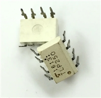
 TLP250光耦合器:资料手册参数分析

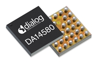
 DA14580 低功耗蓝牙系统级芯片(SoC):资料手册参数分析

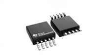
 INA226 高精度电流和功率监控器:资料手册参数分析

 SI2302 N沟道MOSFET:资料手册参数分析
