Absolute Maximum Ratings (Note 1)
If Military/Aerospace specified devices are required,
please contact the National Semiconductor Sales Office/
Distributors for availability and specifications.
Junction Temperature (TJ)
CDIP
175˚C
Recommended Operating
Conditions
Supply Voltage (VCC
)
−0.5V to +7.0V
DC Input Diode Current (IIK
)
Supply Voltage (VCC
)
=
VI −0.5V
−20 mA
+20 mA
’ACT
4.5V to 5.5V
0V to VCC
0V to VCC
=
VI VCC + 0.5V
Input Voltage (VI)
DC Input Voltage (VI)
−0.5V to VCC + 0.5V
Output Voltage (VO
)
DC Output Diode Current (IOK
)
Operating Temperature (TA)
54ACT
=
VO −0.5V
−20 mA
+20 mA
−55˚C to +125˚C
=
VO VCC + 0.5V
Minimum Input Edge Rate (∆V/∆t)
’ACT Devices
DC Output Voltage (VO
DC Output Source
)
−0.5V to VCC + 0.5V
VIN from 0.8V to 2.0V
±
±
or Sink Current (IO
)
50 mA
@
VCC 4.5V, 5.5V
125 mV/ns
DC VCC or Ground Current
per Output Pin (ICC or IGND
Note 1: Absolute maximum ratings are those values beyond which damage
to the device may occur. The databook specifications should be met, without
exception, to ensure that the system design is reliable over its power supply,
temperature, and output/input loading variables. National does not recom-
)
50 mA
Storage Temperature (TSTG
)
−65˚C to +150˚C
™
mend operation of FACT circuits outside databook specifications.
DC Characteristics for ’ACT Family Devices
54ACT
=
Symbol
Parameter
VCC
(V)
TA
Units
Conditions
−55˚C to +125˚C
Guaranteed Limits
=
VIH
Minimum High Level
Input Voltage
4.5
5.5
4.5
5.5
4.5
5.5
2.0
2.0
0.8
0.8
4.4
5.4
V
V
V
VOUT 0.1V
or VCC − 0.1V
=
VIL
Maximum Low Level
Input Voltage
VOUT 0.1V
or VCC − 0.1V
=
VOH
Minimum High Level
Output Voltage
IOUT −50 µA
(Note 2)
=
VIN VIL or VIH
=
IOH −24 mA
4.5
5.5
4.5
5.5
3.70
4.70
0.1
V
V
=
IOH −24 mA
=
VOL
Maximum Low Level
Output Voltage
IOUT 50 µA
0.1
(Note 2)
=
VIN VIL or VIH
=
IOL 24 mA
4.5
5.5
5.5
0.50
0.50
V
=
IOL 24 mA
=
±
IIN
Maximum Input
Leakage Current
Maximum TRI-STATE
Current
1.0
µA
µA
mA
VI VCC, GND
=
±
IOZ
5.5
5.5
5.0
VI VIL, VIH
=
VO VCC, GND
=
VI VCC − 2.1V
ICCT
Maximum ICC/Input
(Note 3)
1.6
=
VOLD 1.65V Max
IOLD
IOHD
ICC
Minimum Dynamic
Output Current
Maximum Quiescent
Supply Current
5.5
5.5
5.5
50
mA
mA
µA
=
VOHD 3.85V Min
−50
80.0
=
VIN VCC
or GND
Note 2: All outputs loaded; thresholds on input associated with output under test.
Note 3: Maximum test duration 2.0 ms, one output loaded at a time.
@ @
I for 54ACT 25˚C is identical to 74ACT 25˚C.
CC
Note 4:
3
www.national.com


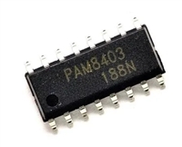
 PAM8403音频功率放大器:资料手册参数分析

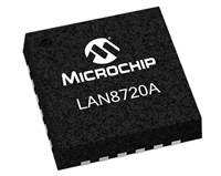
 LAN8720以太网收发器:资料手册参数分析

 SI2301 N沟道MOSFET:资料手册参数分析

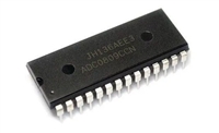
 ADC0809逐次逼近寄存器型模数转换器:资料手册参数分析
