ELECTRICAL CHARACTERISTICS
STATIC ELECTRICAL CHARACTERISTICS
STATIC ELECTRICAL CHARACTERISTICS
Table 4. Static Electrical Characteristics
Characteristics noted under conditions 3.1 V ≤ VDD ≤ 5.25 V, 8.0 V ≤ VPWR ≤ 16 V, -40°C ≤ TC ≤ 125°C, unless otherwise
noted.(7) Where applicable, typical values reflect the parameter’s approximate average value with VPWR = 13 V, TA = 25°C.
Characteristic
Symbol
Min
Typ
Max
Unit
POWER INPUT
Supply Voltage
V
Supply Voltage Range Quasi-functional(8)
Fully Operational
V
V
V
5.5
8.0
26
–
–
–
8.0
26
(
)
PWR QF
PWR(FO)
PWR(QF)
Supply Voltage Range Quasi-functional(8)
38/40
Supply Current
I
mA
PWR(ON)
All Switches Open, Normal Mode, Tri-state Disabled
–
2.0
4.0
Sleep State Supply Current
I
μA
PWR(SS)
Scan Timer = 64 ms, Switches Open
40
70
–
100
Logic Supply Voltage
V
3.1
5.25
V
DD
Logic Supply Current
I
mA
DD
All Switches Open, Normal mode
–
–
0.25
10
0.5
20
Sleep State Logic Supply Current
Scan Timer = 64 ms, Switches Open
I
μA
DD(SS)
SWITCH INPUT
Pulse Wetting Current Switch-to-Battery (Current Sink)
Pulse Wetting Current Switch-to-Ground (Current Source)
Sustain Current Switch-to-Battery Input (Current Sink)
Sustain Current Switch-to-Ground Input (Current Source)
Sustain Current Matching Between Channels on Switch-to-Ground I/Os
I
I
12
12
15
16
18
18
mA
mA
mA
mA
%
PULSE
PULSE
I
1.8
1.8
2.0
2.0
2.2
2.2
SUSTAIN
SUSTAIN
I
I
MATCH
ISUS(MAX)
I
SUS(MIN)
-
–
2.0
4.0
X 100
ISUS(MIN)
Input Offset Current When Selected as Analog
I
-2.0
-10
1.4
2.5
2.0
10
μA
OFFSET
Input Offset Voltage When Selected as Analog
V(SP&SGINPUTS) to AMUX Output
V
mV
OFFSET
Analog Operational Amplifier Output Voltage
V
mV
V
OL
Sink 250μA
–
10
30
Analog Operational Amplifier Output Voltage
V
OH
Source 250μA
V
-0.1
–
–
DD
Switch Detection Threshold
V
3.70
4.0
4.3
V
V
TH
Switch Input Voltage Range
V
IN
33972
-14
-14
–
–
38
40
33972A
Temperature Monitor(9), (10)
Temperature Monitor Hysteresis(10)
Notes
T
155
5.0
–
185
15
°C
°C
LIM
T
10
LIM(HYS)
7.
T is the TCASE of the package
C
8. Device operational. Table parameters may be out of specification.
9. Thermal shutdown of 16 mA pull-up and pulldown current sources only. 2.0 mA current source/sink and all other functions remain active.
10. This parameter is guaranteed by design but is not production tested.
33972
Analog Integrated Circuit Device Data
Freescale Semiconductor
6


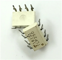
 TLP250光耦合器:资料手册参数分析

 DA14580 低功耗蓝牙系统级芯片(SoC):资料手册参数分析

 INA226 高精度电流和功率监控器:资料手册参数分析

 SI2302 N沟道MOSFET:资料手册参数分析
