Zibo Seno Electronic Engineering Co., Ltd.
SL20T80 - SL20T200
20.0 A SUPER BARRIER RECTIFIER
Features
!
!
!
Schottky Barrier Chip
Bypass Diodes for Solar Panels
ꢀ
TO-277B
High Junction Temperture
High Thermal Reliability
Patented Super Barrier Rectifier Technology
High Foward Surge Capability
Ultra Low Power Loss, High Efficiency
Excellent High Temperature Stability
!
!
!
!
!
1.90
1.70
1.95
1.65
4.20
3.80
5.50
5.30
3.85
3.25
0.65
0.45
Mechanical Data
3.20
2.90
!
!
Case:TO-277B Molded Plastic "Green" Molding Compound
Terminals: Plated Leads Solderable per
MIL-STD-202, Method 208
1.00
0.80
1.20
1.00
!
!
!
!
Polarity: Cathode Band
Weight: 0.093 grams (approx.)
Mounting Position: Any
0.45
0.20
1.20
1.00
6.60
6.40
Marking: Type Number
Lead Free: For RoHS/Lead Free Version
!
Dimensions in millimeters
Maximum Ratings and Electrical Characteristics @TA=25°C unless otherwise specified
Single Phase, half wave, 60Hz, resistive or inductive load.
For capacitive load, derate current by 20%.
SL20T80
80
SL20T100
100
SL20T120
SL20T150
150
SL20T200
200
Characteristic
Symbol
Unit
V
Peak Repetitive Reverse Voltage
Working Peak Reverse Voltage
DC Blocking Voltage
VRRM
VRWM
VR
120
RMS Reverse Voltage
VR(RMS)
IO
56
70
84
20
105
140
V
A
Average Rectified Output Current
(Note 1)
@TL = 100°C
Non-Repetitive Peak Forward Surge Current 8.3ms
Single half sine-wave superimposed on rated load
(JEDEC Method)
IFSM
I2t
300
A
I2t Rating for Fusing (t<8.3ms)
A2s
259.4
Typ. Max.
Typ. Max.
Forward Voltage Drop
@I
0.37
0.45
-
-
0.43
0.60
0.67
-
-
-
= 25°C
= 25°C
= 25°C
= 25°C
F = 1.0A
F = 5.0A
F = 10A
F = 20A
TA
TA
TA
TA
VFM
V
@I
@I
@I
0.51 0.63
0.61 0.66
0.63
0.80
0.75 0.85
0.88
Peak Reverse Current
At Rated DC Blocking Voltage
@TA = 25°C
@TA = 100°C
0.3
15
IRM
mA
Rꢀ
JA
110
°C/W
°C
Typical Thermal Resistance (Note 1)
Operating and Storage Temperature Range
Tj, TSTG
-55 to +150
Note: 1. Valid provided that leads are kept at ambient temperature at a distance of 9.5mm from the case.
2. FR-4 PCB, 2oz. Copper, minimum recommended pad layout .
3. Polymide PCB, 2oz. Copper. Cathode pad dimensions 18.8mm x 14.4mm. Anode pad dimensions 5.6mm x 14.4mm.
www.senocn.com
SL20T80 - SL20T200
1 of 2


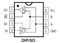
 MAX487芯片引脚图及功能、应用领域详解

 IR2110驱动芯片引脚图及功能、电路图详解

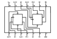
 74LS74是什么芯片 74LS74引脚图及功能表

 CD4511芯片引脚图及功能、电路图解析
