Design Idea DI-89
LinkSwitch®-XT Low Cost 2 W
CV Power Adapter
Application
Device
Power Output
Input Voltage
Output Voltage
Topology
Adapter
LNK362P
2 W
85-265 VAC
6.2 V
Flyback
the ringing of the filter. Switching frequency jitter and
PIʼs E-Shield transformer construction technology enable
this design to meet EN55022 Class-B conducted EMI with
good margin (see Figure 4). Y capacitor C4 (optional) can
improve the unit-to-unit repeatability of EMI scans.
Design Highlights
•
•
Low-cost, low parts-count CV solution: 20 components
Proprietary IC design and winding techniques enable a
Clampless™ drain-node
•
± 5% over-temperature threshold – with hysteretic
recovery – keeps PCB temperatures below safety limits
Auto-restart: output short circuit and open loop protection
IC creepage > 3.2 mm: no arcing in humid environments
Easily meets all EPS energy efficiency standards
Meets CISPR-22 Class B EMI with sufficient margin
ThissupplyalsotakesadvantageofPIʼsClamplesstransformer
techniques, which uses T1ʼs primary winding capacitance to
clamp the voltage spike that its leakage inductance causes,
each time the MOSFET in U1 turns off. Therefore, this
converter has no primary clamp components connected to
the drain-node.
•
•
•
•
Operation
Fromno-loaduntilmaximumoutputpower(2W)isdelivered,
the LNK362P (U1) regulates the output voltage by skipping
switching cycles, based on the current delivered into the
feedback(FB)pin. Iftheoutputisoverloadedandnofeedback
(<49µA)isreceivedwithina40msperiod,U1goesintoauto-
restart mode. In auto-restart, MOSFET switching is enabled
for about 40 ms approximately every 800 ms if no feedback
is received within the 40 ms window of enabled switching.
ThisLinkSwitch-XTbasedflybackconverter(Figure1)provides
2 W of tightly regulated constant voltage (CV) output power,
while meeting the active-mode efficiency and no-load power
consumption requirements of all harmonized energy efficiency
(EPA, CEC) standards (see Figure 2 and Figure 3).
DiodesD1–D4rectifytheACinput. TheresultingDCisfiltered
by bulk storage capacitors C1 and C2. Components L1, L2, C1
and C2 form a conducted EMI noise filter. Resistor R1 dampens
C4*
100 pF
250 VAC
C5
L1
6.2 V,
330 µF
T1
1 mH
322 mA
16 V
EE16
4
5
9
8
J3-1
J3-2
D5
1N4934
3
NC NC
RF1
8.2 k
2.5 W
VR1
D1
D2
R1
3.9 k
1/8 W
BZX79-
B5V1
1N4005 1N4005
J1
5.1 V, 2%
R3
390 Ω
1/8 W
C1
3.3 µF
400 V
C2
3.3 µF
400 V
85-265
VRMS
R2
1 k
1/8 W
U2
PC817A
J2
D
S
FB
BP
LinkSwitch-XT
U1
LNK362P
*Optional component
D3
D4
C3
100 nF
50 V
1N4005 1N4005
L2
1 mH
PI-4205-110805
Figure 1. LNK362 Based 6.2 V, 322 mA, 2 W, Low-cost, Flyback CV Output Power Adapter.
November 2005
DI-89
www.powerint.com

 5秒后页面跳转


 CR6842芯片参数、引脚配置、应用电路图详解

 国产PoE供电芯片选型替代指南,你想要的都在这里!
 LM2596可调稳压器引脚功能及电路原理图
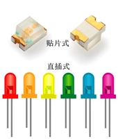 一文详解发光二极管(LED)特性及电路应用


 浙公网安备 33010502006866号 浙ICP备10014259号-119
营业执照ICP证
浙公网安备 33010502006866号 浙ICP备10014259号-119
营业执照ICP证


