Design Idea DI-58
LinkSwitch Low Cost 1.5 W
CV/CC Charger or Adapter
Topology
Device
Power Output
Input Voltage
Output Voltage
Application
Flyback
Charger/Adapter
1.5 W
85-265 VAC
LNK500
5.5 V
LinkSwitchderivesallfeedbackinformationfromtheprimary.
During output diode conduction, the output voltage reflected
through the turns ratio is sampled and held by C4. The
feedback voltage across C4 (VOR) is converted into feedback
currentbyR2andfedintotheCONTROLpin. Thisfeedback
current regulates the output by PWM control during CV
operation, and by reducing the internal current limit during
CC operation. Below an output voltage of ~2 V, LinkSwitch
enters auto-restart, limiting average output current to less
than 50 mA. The nominal transition from CV to CC occurs
at 5.5 V, 0.27 A. The output envelope characteristic and
specification limits are shown in Figure 2.
Design Highlights
• Replaces a linear transformer based supply at the same or
lower cost but with much higher performance
• <0.3Wconsumptionatzeroloadmeetsworldwideguidelines
(EC’s 0.3 W, USA’s 1 W for example)
• Extremely simple circuit – only 15 components for
production-worthy design
• Primary based CV/CC output – no secondary sense
components required
• ±10% output voltage and ±25% output current tolerances at
peak power point
• Fullyprotectedforthermal,shortcircuitandopenloopfaults
• >62% efficiency (>70% with R1 replaced by an inductor)
• Meets CISPR22B/EN55022B EMI limits with low cost
resistive input filter
• Ultra-low leakage current design <5 µA
• EE13 core for low cost and small size
TogetherwithD3,C4andR2arealsopartoftheprimaryclamp,
limiting the peak drain to source voltage due to leakage
inductance. Resistor R3 filters the leading edge leakage
inductance spike, reducing the error in the feedback voltage.
The CONTROL pin capacitor C3 provides energy storage for
supply start-up and sets auto-restart timing during fault
conditions.
Operation
The AC input is rectified and filtered by D1, D2, C1 and C2.
Conducted EMI filter is provided both by a π filter (C1, R1 and
C2) and a differential filter (RF1 and C1). Together with a
shield in the transformer (formed from part of the primary), the
designmeetsconductedEMIlimitswithnoY-capacitorbetween
primary and secondary. Resistor RF1 also functions as a fuse.
Key Design Points
•
Select transformer turns ratio to give a VOR of 40 V
to 60 V. Lower values reduce power capability; higher
values increase no-load consumption.
• R2 provides 2.3 mA into the CONTROL pin at the peak
power point at 85 VAC. The value can be adjusted to
center the output voltage.
R1
68 Ω
Flameproof
LinkSwitch
T1
5.5 V, 0.27 A
D
S
1
C
U1
LNK500
5
6
104T
C3
0.22 µF
34 AWG
15 T
30 AWG
T.I.W.
C5
D1
1N4007
4
220 µF
12T
C4
RF1
10 Ω
Fusible
16V
2 x 30 AWG
0.1 µF
100 V
FILM
R2
21 kΩ
L
RTN
3
C1, C2
2.2 µF
400 V
85-265
VAC
EE13
D4
D3
1N4937
LP = 1.36 mH UF4002
1A 100V
N
D2
1N4007
R3
100 Ω
PI-3687-091903
Figure 1. LinkSwitch 1.5 W Charger Power Supply: 85 VAC to 265 VAC Input, 5.5 V, 0.27 A Output
September 2003
DI-58
www.powerint.com


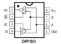
 MAX487芯片引脚图及功能、应用领域详解

 IR2110驱动芯片引脚图及功能、电路图详解

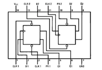
 74LS74是什么芯片 74LS74引脚图及功能表

 CD4511芯片引脚图及功能、电路图解析
