Data Sheet
June 1999
ORCA® Series 3C and 3T
Field-Programmable Gate Arrays
logic cell (PLC), with over 50% speed improvement typi-
cal.
Features
■ Abundant hierarchical routing resources based on rout-
ing two data nibbles and two control lines per set provide
for faster place and route implementations and less rout-
ing delay.
■ High-performance, cost-effective, 0.35 µm (OR3C) and
0.3 µm (OR3T) 4-level metal technology, (4- or 5-input
look-up table delay of 1.1 ns with -7 speed grade in
0.3 µm).
■ TTL or CMOS input levels programmable per pin for the
■ Same basic architecture as lower-voltage, advanced
process technology Series 3 architectures. (See ORCA
Series 3L FPGA documentation.)
OR3Cxx (5.0 V) devices.
■ Individually programmable drive capability:
12 mA sink/6 mA source or 6 mA sink/3 mA source.
■ Up to 186,000 usable gates.
■ Built-in boundary scan (IEEE †1149.1 JTAG) and
■ Up to 452 user I/Os. (OR3Txxx I/Os are 5 V tolerant to
allow interconnection to both 3.3 V and 5 V devices,
selectable on a per-pin basis.)
TS_ALL testability function to 3-state all I/O pins.
■ Enhanced system clock routing for low skew, high-speed
clocks originating on-chip or at any I/O.
■ Pin selectable I/O clamping diodes provide 5 V or 3.3 V
PCI compliance and 5 V tolerance on OR3Txxx devices.
■ Up to four ExpressCLK inputs allow extremely fast clock-
ing of signals on- and off-chip plus access to internal
general clock routing.
■ Twin-quad programmable function unit (PFU) architec-
ture with eight 16-bit look-up tables (LUTs) per PFU,
organized in two nibbles for use in nibble- or byte-wide
functions. Allows for mixed arithmetic and logic functions
in a single PFU.
■ StopCLK feature to glitchlessly stop/start ExpressCLKs
independently by user command.
■ Programmable I/O (PIO) has:
■ Nine user registers per PFU, one following each LUT,
plus one extra. All have programmable clock enable and
local set/reset, plus a global set/reset that can be dis-
abled per PFU.
— Fast-capture input latch and input flip-flop (FF) latch
for reduced input setup time and zero hold time.
— Capability to (de)multiplex I/O signals.
— Fast access to SLIC for decodes and PAL-like
functions.
■ Flexible input structure (FINS) of the PFUs provides a
routability enhancement for LUTs with shared inputs and
the logic flexibility of LUTs with independent inputs.
— Output FF and two-signal function generator to
reduce CLK to output propagation delay.
— Fast open-drain dive capability
■ Fast-carry logic and routing to adjacent PFUs for nibble-,
byte-wide, or longer arithmetic functions, with the option
to register the PFU carry-out.
— Capability to register 3-state enable signal.
■ Baseline FPGA family used in Series 3+ FPSCs (field
programmable system chips) which combine FPGA logic
and standard cell logic on one device.
■ Softwired LUTs (SWL) allow fast cascading of up to
three levels of LUT logic in a single PFU for up to 40%
speed improvement.
* PAL is a trademark of Advanced Micro Devices, Inc.
†IEEE is a registered trademark of The Institute of Electrical and
Electronics Engineers, Inc.
■ Supplemental logic and interconnect cell (SLIC) provides
3-statable buffers, up to 10-bit decoder, and PAL*-like
AND-OR with optional INVERT in each programmable
Table 1. ORCA Series 3 (3C and 3T) FPGAs
System
Process
Device
LUTs
Registers Max User RAM User I/Os Array Size
Gates‡
36K
Technology
0.3 µm/4 LM
0.3 µm/4 LM
0.3 µm/4 LM
0.3 µm/4 LM
0.3 µm/4 LM
OR3T20
OR3T30
1152
1568
2592
3872
6272
1872
2436
3780
5412
8400
18K
25K
42K
62K
100K
196
228
292
356
452
12 x 12
14 x 14
18 x 18
22 x 22
28 x 28
48K
OR3C/3T55
OR3C/3T80
OR3T125
80K
116K
186K
‡The system gate counts range from a logic-only gate count to a gate count assuming 30% of the PFUs/SLICs being used as RAMs.
The logic-only gate count includes each PFU/SLIC (counted as 108 gates per PFU/SLIC), including 12 gates per LUT/FF pair (eight per
PFU), and 12 gates per SLIC/FF pair (one per PFU). Each of the four PIOs per PIC is counted as 16 gates (two FFs, fast-capture latch,
output logic, CLK drivers, and I/O buffers). PFUs used as RAM are counted at four gates per bit, with each PFU capable of implementing
a 32 x 4 RAM (or 512 gates) per PFU.

 5秒后页面跳转


 NE5532双低噪声运算放大器:资料手册参数分析

 74LS138 3-to-8线解码器/多路复用器:资料手册参数分析
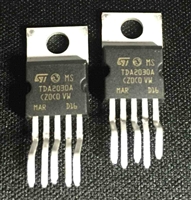 TDA2030音频功率放大器:资料手册参数分析
 74HC595移位寄存器芯片:参数深入解析与应用实践指南


 浙公网安备 33010502006866号 浙ICP备10014259号-119
营业执照ICP证
浙公网安备 33010502006866号 浙ICP备10014259号-119
营业执照ICP证


