June 1999
N
CLC5612
Dual, High Output, Programmable Gain Buffer
General Description
Features
■
The CLC5612 is a dual, low-cost, high-speed (90MHz) buffer
which features user-programmable gains of +2, +1, and
-1V/V. The CLC5612 also has a new output stage that delivers
high output drive current (130mA), but consumes minimal
quiescent supply current (1.5mA/ch) from a single 5V supply. Its
current feedback architecture, fabricated in an advanced comple-
mentary bipolar process, maintains consistent performance over
a wide range of gains and signal levels, and has a linear-phase
response up to one half of the -3dB frequency.
130mA output current
■
0.15%, 0.02° differential gain, phase
1.5mA/ch supply current
■
■
■
■
■
■
■
90MHz bandwidth (A = +2)
v
-87/-93dBc HD2/HD3 (1MHz)
17ns settling to 0.05%
290V/µs slew rate
Stable for capacitive loads up to 1000pf
Single 5V to ±5V supplies
The CLC5612 offers 0.1dB gain flatness to 18MHz and differen-
tial gain and phase errors of 0.15% and 0.02°. These features are
ideal for professional and consumer video applications.
Applications
■
Video line driver
■
Coaxial cable driver
■
Twisted pair driver
The CLC5612 offers superior dynamic performance with a
90MHz small-signal bandwidth, 290V/µs slew rate and 6.2ns
■
Transformer/coil driver
High capacitive load driver
Portable/battery-powered applications
A/D driver
■
rise/fall times (2V
). The combination of low quiescent power,
step
■
high output current drive, and high-speed performance make
the CLC5612 well suited for many battery-powered personal
communication/computing systems.
■
Maximum Output Voltage vs. RL
10
The ability to drive low-impedance, highly capacitive loads,
makes the CLC5612 ideal for single ended cable applications.
It also drives low impedance loads with minimum distortion.
The CLC5612 will drive a 100Ω load with only -74/-86dBc
9
8
VCC = ±5V
7
6
5
4
second/third harmonic distortion (A = +2, V = 2V , f = 1MHz).
v
out
pp
With a 25Ω load, and the same conditions, it produces only -70/
-67dBc second/third harmonic distortion. It is also optimized for
driving high currents into single-ended transformers and coils.
3
Vs = +5V
2
1
When driving the input of high-resolution A/D converters, the
CLC5612 provides excellent -87/-93dBc second/third harmonic
10
100
1000
RL (Ω)
distortion (A = +2, V
= 2V , f = 1MHz, R = 1kΩ) and fast
v
out
pp
L
settling time.
Typical Application
Differential Line Driver with Load Impedance Conversion
Rm/2
Pinout
Io
1:n
+
Vo
-
Zo
DIP & SOIC
Req
RL
Vd/2
UTP
1
8
7
6
5
OUT1
-IN1
+VCC
Rm/2
-Vd/2
1kΩ
1kΩ
1kΩ
-
1kΩ
-
2
3
4
OUT2
-IN2
+
+
Vin
1kΩ
-
1kΩ
+IN1
-VCC
1kΩ
-
1kΩ
Rt
+
+
+IN2
Rt2
CLC5612
Note: Supplies and bypassing not shown.
© 1999 National Semiconductor Corporation
Printed in the U.S.A.
http://www.national.com

 5秒后页面跳转


 74LS74是什么芯片 74LS74引脚图及功能表

 CD4511芯片引脚图及功能、电路图解析
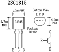 2SC1815三极管参数及引脚图功能详解
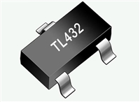 TL432和TL431有什么区别


 浙公网安备 33010502006866号 浙ICP备10014259号-119
营业执照ICP证
浙公网安备 33010502006866号 浙ICP备10014259号-119
营业执照ICP证


