DC-6.0 GHz InGaP HBT, MMIC or Packaged,
Matched Gain Block Amplifier
May 2006 - Rev 23-May-06
CGB7001-SC (-BD)
Features
Functional Block Diagram (SOT-89)
Low Operating Voltage: 5V
Ground
4
28.0 dBm Output IP3 @ 850 MHz
3.3 dB Noise Figure @ 850 MHz
20.5 dB Gain @ 850 MHz
14.2 dBm P1dB @ 850 MHz
2
3
1
Low Performance Variation Over Temperature
Low Cost: Die Form or SOT-89 Package
100% DC On-Wafer Testing
ESD Protection on All Die: >1000V HBM
Low Thermal Resistance: <110ºC/Watt
Ground Output
Bias
Input
Absolute Maximum Ratings
Max Device Voltage
Max Device Current
Max Device Dissipated Power
RF Input Power
+5.5 V
110 mA
Applications
0.45 W
PA Driver Amp, IF Amp, LO Buffer Amp
Cellular, PCS, GSM, UMTS
Wireless Data and SATCOM
Transmit and Receive Functions
CATV
+17 dBm
-55ºC to 150ºC
150ºC
Storage Temperature
Junction Temperature
Operating Temperature
Thermal Resistance
EDS (HBM)
-40ºC to +85ºC
110º C/W
1000 V
Operation of this device above any of these parameters may cause
permanent damage.
Description
The CGB7001-SC (-BD) is a Darlington Configured,
high dynamic range, utility gain block amplifier. Designed for
applications operating within the DC to 6.0 GHz frequency
range, Mimix’s broadband, cascadable, gain block amplifiers are
ideal solutions for transmit, receive and IF applications.
These MMIC amplifiers are available in bare die form
thermally robust and reliable gain block solution.
The InGaP HBT die have extra pads to enable
thorough DC testing. This unique test capability and the
inclusion of ESD protection on all die, significantly enhances
the quality, reliability and ruggedness of these products.
With a single bypass capacitor, optional RF choke
or an industry standard SOT-89 package. Mimix's InGaP HBT
technology and an industry low thermal resistance offers a
and two DC blocking capacitors, this gain block amplifier
offers significant ease of use in a broad range of applications.
Electrical Characteristics
Unless otherwise specified, the following specifications are guaranteed at room temperature in a Mimix test fixture.
850 MHz
Typ.
1950 MHz
Typ.
2400 MHz
Typ.
3500 MHz
Typ.
Parameter
Temperature (ºC)
Min.
Max.
Min.
Max.
Min.
Max.
Min.
Max.
Units
Small Signal Gain
+25
-40 to +85
+25
-40 to +85
+25
-40 to +85
+25
-40 to +85
+25
-40 to +85
+25
-40 to +85
+25
-40 to +85
+25
-40 to +85
19.5 20.5 21.5 16.8 17.8 18.8 16.0 17.0 18.0
19.2 20.5 21.8 16.5 17.8 19.1 17.0 17.0 18.3
14.8
14.8
11.1
11.1
24.0
24.0
3.8
3.8
35
35
15
dB
dB
Output P1dB
13.2 14.2
11.5 14.2
26.5 28.0
25.0 28.0
3.3
12.5 13.5
11.0 13.5
25.5 27.0
24.0 27.0
3.5
12.1 13.1
11.0 13.1
25.0 26.5
24.0 26.5
3.6
dBm
dBm
dBm
dBm
dB
Output IP3
Noise Figure
4.1
4.4
39
4.3
4.7
39
4.4
4.8
38
3.3
3.5
3.6
dB
Operating Current
Input Return Loss
Output Return Loss
32
28
12
11
18
17
35
35
16
16
23
32
28
11
10
13
12
35
35
15
15
18
32
28
11
10
13
12
35
35
15
15
18
18
mA
mA
dB
dB
dB
dB
dBm
dBm
43
43
42
15
15
15
23
18
Pout @ -45 dBc, ACP
IS-95, 9 Forward Channels
10.0
9.0
10.0
10.0
Notes: 1. Test Conditions in Mimix eval board, Vs = 5 V, Id = 35 mA Typ., Rbias = 27 , Zs = Zl = 50 , OIP3 tone spacing = 1 MHz, Pout per tone = 3 dBm.
2. Values reflect performance in recommended application circuit.
Page 1 of 7
Mimix Broadband, Inc., 10795 Rockley Rd., Houston,Texas 77099
Tel: 281.988.4600 Fax: 281.988.4615 mimixbroadband.com
Characteristic Data and Specifications are subject to change without notice. ©2006 Mimix Broadband, Inc.
Export of this item may require appropriate export licensing from the U.S. Government. In purchasing these parts, U.S. Domestic customers accept
their obligation to be compliant with U.S. Export Laws.

 5秒后页面跳转


 74LS74是什么芯片 74LS74引脚图及功能表

 CD4511芯片引脚图及功能、电路图解析
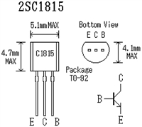 2SC1815三极管参数及引脚图功能详解
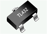 TL432和TL431有什么区别


 浙公网安备 33010502006866号 浙ICP备10014259号-119
营业执照ICP证
浙公网安备 33010502006866号 浙ICP备10014259号-119
营业执照ICP证


