
 5秒后页面跳转

| 生命周期: | Obsolete | 零件包装代码: | LCC |
| 包装说明: | QCCN, | 针数: | 44 |
| Reach Compliance Code: | unknown | HTS代码: | 8542.31.00.01 |
| 风险等级: | 5.75 | Is Samacsys: | N |
| 地址总线宽度: | 边界扫描: | NO | |
| 最大时钟频率: | 1 MHz | 数据编码/解码方法: | NRZ |
| 最大数据传输速率: | 0.01220703125 MBps | 外部数据总线宽度: | 16 |
| JESD-30 代码: | S-CQCC-N44 | JESD-609代码: | e0 |
| 长度: | 16.535 mm | 低功率模式: | YES |
| 串行 I/O 数: | 1 | 端子数量: | 44 |
| 最高工作温度: | 125 °C | 最低工作温度: | -55 °C |
| 封装主体材料: | CERAMIC, METAL-SEALED COFIRED | 封装代码: | QCCN |
| 封装形状: | SQUARE | 封装形式: | CHIP CARRIER |
| 认证状态: | Not Qualified | 筛选级别: | MIL-STD-883 |
| 座面最大高度: | 3.05 mm | 最大供电电压: | 5.25 V |
| 最小供电电压: | 4.75 V | 标称供电电压: | 5 V |
| 表面贴装: | YES | 技术: | CMOS |
| 温度等级: | MILITARY | 端子面层: | TIN LEAD |
| 端子形式: | NO LEAD | 端子节距: | 1.27 mm |
| 端子位置: | QUAD | 宽度: | 16.535 mm |
| uPs/uCs/外围集成电路类型: | SERIAL IO/COMMUNICATION CONTROLLER, SERIAL | Base Number Matches: | 1 |
| 型号 | 品牌 | 描述 | 获取价格 | 数据表 |
| 5962-8688001XX | WEDC | Serial I/O Controller, 1 Channel(s), 0.01220703125MBps, CMOS, CQCC44, CERAMIC, LCC-44 |
获取价格 |

|
| 5962-8688002QA | ETC | Transceiver |
获取价格 |
|
| 5962-8688002XA | ETC | Transceiver |
获取价格 |
|
| 5962-86881012A | TI | LS SERIES, 4-BIT ARITHMETIC LOGIC UNIT, QCC20, 0.350 X 0.350 INCH, CC-20 |
获取价格 |
|
| 5962-86881012C | ETC | Fixed Point ALU |
获取价格 |
|
| 5962-8688101RA | TI | LS SERIES, 4-BIT ARITHMETIC LOGIC UNIT, DIP20, 0.250 X 1.0625 INCH, DIP-20 |
获取价格 |
|
 74LS74是什么芯片 74LS74引脚图及功能表

 CD4511芯片引脚图及功能、电路图解析
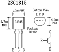 2SC1815三极管参数及引脚图功能详解
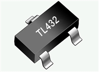 TL432和TL431有什么区别
工作时间:9:00-21:00
CEO邮箱:ceo@jiepei.com
投诉邮箱:tousu@jiepei.com


 浙公网安备 33010502006866号 浙ICP备10014259号-119
营业执照ICP证
浙公网安备 33010502006866号 浙ICP备10014259号-119
营业执照ICP证


