
 5秒后页面跳转

| 型号 | 品牌 | 描述 | 获取价格 | 数据表 |
| GJ122 | GTM | NPN EPITAXIAL PLANAR TRANSISTOR |
获取价格 |

|
| GJ127 | GTM | NPN EPITAXIAL PLANAR TRANSISTOR |
获取价格 |
|
| GJ12M | ETC | PROBE WITH OVEN CLIP |
获取价格 |
|
| GJ1386 | GTM | PNP EPITAXIAL SILICON TRANSISTOR |
获取价格 |
|
| GJ15N03 | GTM | N-CHANNEL ENHANCEMENT MODE POWER MOSFET |
获取价格 |
|
| GJ15T03 | GTM | N-CHANNEL ENHANCEMENT MODE POWER MOSFET |
获取价格 |
|
 CR6842芯片参数、引脚配置、应用电路图详解

 国产PoE供电芯片选型替代指南,你想要的都在这里!
 LM2596可调稳压器引脚功能及电路原理图
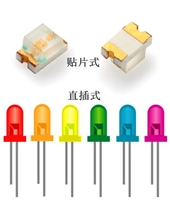 一文详解发光二极管(LED)特性及电路应用
工作时间:9:00-21:00
CEO邮箱:ceo@jiepei.com
投诉邮箱:tousu@jiepei.com


 浙公网安备 33010502006866号 浙ICP备10014259号-119
营业执照ICP证
浙公网安备 33010502006866号 浙ICP备10014259号-119
营业执照ICP证


