
 5秒后页面跳转

| 是否Rohs认证: | 不符合 | 生命周期: | Transferred |
| Reach Compliance Code: | unknown | 风险等级: | 5.8 |
| Is Samacsys: | N | JESD-609代码: | e0 |
| 安装特点: | THROUGH HOLE MOUNT | 最高工作温度: | 70 °C |
| 最低工作温度: | 像素大小: | 13X11 µm | |
| 电源: | 15 V | 子类别: | CCD Image Sensors |
| 表面贴装: | NO | 端子面层: | Tin/Lead (Sn/Pb) |
| Base Number Matches: | 1 |
| 型号 | 品牌 | 描述 | 获取价格 | 数据表 |
| TH7852ACCA | ATMEL | CCD Sensor, 0.40-0.75V, Rectangular, Through Hole Mount, DIP-24 |
获取价格 |

|
| TH7852AVCM | ATMEL | CCD Sensor, 0.40-0.75V, Rectangular, Through Hole Mount, DIP-24 |
获取价格 |
|
| TH7852CD | ETC | TABLEAU RESUME DES DTC MATRICIELS |
获取价格 |
|
| TH786 | ETC | 共模电感 |
获取价格 |
|
| TH7861CD | ETC | Area Array Charge-Coupled Device(CCD) Image Sensors |
获取价格 |
|
| TH7862ACD | ETC | Area Array Charge-Coupled Device(CCD) Image Sensors |
获取价格 |
|
 CR6842芯片参数、引脚配置、应用电路图详解

 国产PoE供电芯片选型替代指南,你想要的都在这里!
 LM2596可调稳压器引脚功能及电路原理图
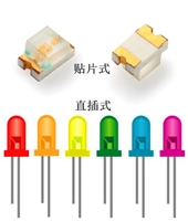 一文详解发光二极管(LED)特性及电路应用
工作时间:9:00-21:00
CEO邮箱:ceo@jiepei.com
投诉邮箱:tousu@jiepei.com


 浙公网安备 33010502006866号 浙ICP备10014259号-119
营业执照ICP证
浙公网安备 33010502006866号 浙ICP备10014259号-119
营业执照ICP证


