Differential/Single-Ended Input, Dual
2 MSPS, 12-Bit, 3-Channel SAR ADC
AD7266
FUNCTIONAL BLOCK DIAGRAM
FEATURES
REF SELECT
D
A
AV
DV
CAP
DD
DD
Dual 12-bit, 3-channel ADC
Throughput rate: 2 MSPS
BUF
T/H
REF
Specified for VDD of 2.7 V to 5.25 V
Power consumption
AD7266
V
V
A1
9 mW at 1.5 MSPS with 3 V supplies
27 mW at 2 MSPS with 5 V supplies
Pin-configurable analog inputs
12-channel single-ended inputs
6-channel fully differential inputs
6-channel pseudo differential inputs
70 dB SNR at 50 kHz input frequency
Accurate on-chip reference: 2.5 V
0.2ꢀ maximum @ 25°C, 20 ppm/°C maximum
Dual conversion with read 437.5 ns, 32 MHz SCLK
High speed serial interface
SPI®-/QSPI™-/MICROWIRE™-/DSP-compatible
−40°C to +125°C operation
Shutdown mode: 1 μA maximum
32-lead LFCSP and 32-lead TQFP
1 MSPS version, AD7265
A2
12-BIT
V
V
A3
SUCCESSIVE
APPROXIMATION
ADC
OUTPUT
DRIVERS
MUX
D
A
OUT
A4
V
V
A5
SCLK
CS
RANGE
SGL/DIFF
A0
A6
CONTROL
LOGIC
A1
A2
V
V
B1
B2
V
DRIVE
V
V
B3
MUX
12-BIT
SUCCESSIVE
APPROXIMATION
ADC
OUTPUT
DRIVERS
B4
D
B
T/H
OUT
V
V
B5
B6
BUF
AGND AGND AGND
D
B
DGND
DGND
CAP
GENERAL DESCRIPTION
Figure 1.
The AD72661 is a dual, 12-bit, high speed, low power, successive
approximation ADC that operates from a single 2.7 V to 5.25 V
power supply and features throughput rates up to 2 MSPS. The
device contains two ADCs, each preceded by a 3-channel
multiplexer, and a low noise, wide bandwidth track-and-hold
amplifier that can handle input frequencies in excess of 30 MHz.
The AD7266 is available in a 32-lead LFCSP and a
32-lead TQFP.
PRODUCT HIGHLIGHTS
1. Two Complete ADC Functions Allow Simultaneous
Sampling and Conversion of Two Channels.
The conversion process and data acquisition use standard
control inputs allowing easy interfacing to microprocessors or
DSPs. The input signal is sampled on the falling edge of
conversion is also initiated at this point. The conversion time is
determined by the SCLK frequency. There are no pipelined
delays associated with the part.
Each ADC has three fully/pseudo differential pairs, or six
single-ended channels, as programmed. The conversion
result of both channels is simultaneously available on
separate data lines, or in succession on one data line if only
one serial port is available.
CS
;
2. High Throughput with Low Power Consumption.
The AD7266 offers a 1.5 MSPS throughput rate with 11.4 mW
maximum power dissipation when operating at 3 V.
3. The AD7266 offers both a standard 0 V to VREF input range
and a 2 × VREF input range.
The AD7266 uses advanced design techniques to achieve very
low power dissipation at high throughput rates. With 5 V
supplies and a 2 MSPS throughput rate, the part consumes
6.2 mA maximum. The part also offers flexible power/
throughput rate management when operating in normal mode
as the quiescent current consumption is so low.
4. No Pipeline Delay.
The part features two standard successive approximation
ADCs with accurate control of the sampling instant via a
The analog input range for the part can be selected to be a 0 V
to VREF (or 2 × VREF) range, with either straight binary or twos
complement output coding. The AD7266 has an on-chip 2.5 V
reference that can be overdriven when an external reference is
CS
input and once off conversion control.
1 Protected by U.S. Patent No. 6,681,332
preferred. This external reference range is 100 mV to VDD
.
Rev. B
Information furnished by Analog Devices is believed to be accurate and reliable. However, no
responsibility is assumed by Analog Devices for its use, nor for any infringements of patents or other
rights of third parties that may result from its use. Specifications subject to change without notice. No
license is granted by implication or otherwise under any patent or patent rights of Analog Devices.
Trademarks and registeredtrademarks arethe property of their respective owners.
One Technology Way, P.O. Box 9106, Norwood, MA 02062-9106, U.S.A.
Tel: 781.329.4700
www.analog.com
Fax: 781.461.3113 ©2005–2011 Analog Devices, Inc. All rights reserved.


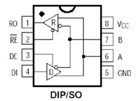
 MAX487芯片引脚图及功能、应用领域详解

 IR2110驱动芯片引脚图及功能、电路图详解

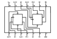
 74LS74是什么芯片 74LS74引脚图及功能表

 CD4511芯片引脚图及功能、电路图解析
