
 5秒后页面跳转

| Source Url Status Check Date: | 2013-05-01 14:56:11.789 | 是否无铅: | 含铅 |
| 是否Rohs认证: | 不符合 | 生命周期: | Obsolete |
| 零件包装代码: | TSSOP | 包装说明: | TSSOP, TSSOP16,.25 |
| 针数: | 16 | Reach Compliance Code: | not_compliant |
| ECCN代码: | EAR99 | HTS代码: | 8542.39.00.01 |
| 风险等级: | 5.37 | Is Samacsys: | N |
| 最大模拟输出电压: | 5.499 V | 最小模拟输出电压: | 0.001 V |
| 转换器类型: | D/A CONVERTER | 输入位码: | BINARY |
| 输入格式: | SERIAL | JESD-30 代码: | R-PDSO-G16 |
| JESD-609代码: | e0 | 长度: | 5 mm |
| 最大线性误差 (EL): | 0.3906% | 湿度敏感等级: | 1 |
| 位数: | 8 | 功能数量: | 1 |
| 端子数量: | 16 | 最高工作温度: | 105 °C |
| 最低工作温度: | -40 °C | 封装主体材料: | PLASTIC/EPOXY |
| 封装代码: | TSSOP | 封装等效代码: | TSSOP16,.25 |
| 封装形状: | RECTANGULAR | 封装形式: | SMALL OUTLINE, THIN PROFILE, SHRINK PITCH |
| 峰值回流温度(摄氏度): | 240 | 电源: | 3/5 V |
| 认证状态: | Not Qualified | 座面最大高度: | 1.2 mm |
| 最大稳定时间: | 8 µs | 标称安定时间 (tstl): | 6 µs |
| 子类别: | Other Converters | 最大压摆率: | 0.9 mA |
| 标称供电电压: | 3 V | 表面贴装: | YES |
| 技术: | CMOS | 温度等级: | INDUSTRIAL |
| 端子面层: | Tin/Lead (Sn85Pb15) | 端子形式: | GULL WING |
| 端子节距: | 0.65 mm | 端子位置: | DUAL |
| 处于峰值回流温度下的最长时间: | 30 | 宽度: | 4.4 mm |
| Base Number Matches: | 1 |
| 型号 | 品牌 | 描述 | 获取价格 | 数据表 |
| AD5306ARUZ | ADI | 暂无描述 |
获取价格 |

|
| AD5306ARUZ1 | ADI | 2.5 V to 5.5 V, 400 μA, 2-Wire Interface, Qu |
获取价格 |
|
| AD5306ARUZ-REEL7 | ADI | 2.5 V to 5.5 V, 400 µA, 2-Wire Interface Quad Voltage Output 8-Bit DAC |
获取价格 |
|
| AD5306ARUZ-REEL71 | ADI | 2.5 V to 5.5 V, 400 μA, 2-Wire Interface, Qu |
获取价格 |
|
| AD5306BRU | ADI | 2.5 V to 5.5 V, 400 μA, 2-Wire Interface, Qu |
获取价格 |
|
| AD5306BRU | ROCHESTER | SERIAL INPUT LOADING, 6 us SETTLING TIME, 8-BIT DAC, PDSO16, MO-153-AB, TSSOP-16 |
获取价格 |
|
 74LS74是什么芯片 74LS74引脚图及功能表

 CD4511芯片引脚图及功能、电路图解析
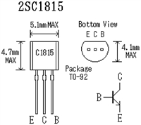 2SC1815三极管参数及引脚图功能详解
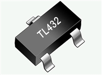 TL432和TL431有什么区别
工作时间:9:00-21:00
CEO邮箱:ceo@jiepei.com
投诉邮箱:tousu@jiepei.com


 浙公网安备 33010502006866号 浙ICP备10014259号-119
营业执照ICP证
浙公网安备 33010502006866号 浙ICP备10014259号-119
营业执照ICP证


