Fully Accurate, 12-/14-/16-Bit, Dual, VOUT
nanoDAC SPI Interface, 4.5 V to 5.5 V in a TSSOP
AD5025/AD5045/AD5065
ence buffer is provided on chip. The AD5025/AD5045/AD5065
incorporate a power-on reset circuit that ensures the DAC output
FEATURES
Low power dual 12-/14-/16-bit DAC, 1 LSB INL
Individual voltage reference pins
Rail-to-rail operation
4.5 V to 5.5 V power supply
Power-on reset to zero scale or midscale
Power down to 400 nA @ 5 V
3 power-down functions
Per channel power-down
Low glitch upon power-up
Hardware power-down lockout capability
Hardware LDAC with software LDAC override function
CLR function to programmable code
SDO daisy-chaining option
powers up zero scale or midscale and remains there until a valid
write takes place to the device. The AD5025/AD5045/AD5065
contain a power-down feature that reduces the current consump-
tion of the device to typically 400 nA at 5 V and provides software
selectable output loads while in power-down mode. The parts are
put into power-down mode over the serial interface. Total unad-
justed error for the parts is <2.5 mV. The parts exhibit very low
glitch on power-up. The outputs of all DACs can be updated
LDAC
simultaneously using the
functionality of user-selectable DAC channels to simultaneously
CLR
function, with the added
update. There is also an asynchronous
to a software-selectable code—0 V, midscale, or full scale. The
PDL
that clears all DACs
parts also feature a power-down lockout pin,
, which can be
14-lead TSSOP
used to prevent the DAC from entering power-down under any
circumstances over the serial interface.
APPLICATIONS
Process controls
Data acquisition systems
PRODUCT HIGHLIGHTS
1. Dual channel available in a 14-lead TSSOP package with
individual voltage reference pins.
2. 12-/14-/16-bit accurate, 1 LSB INL.
Portable battery-powered instruments
Digital gain and offset adjustment
Programmable voltage and current sources
Programmable attenuators
3. Low glitch on power-up.
4. High speed serial interface with clock speeds up to 50 MHz.
5. Three power-down modes available to the user.
6. Reset to known output voltage (zero scale or midscale).
7. Power-down lockout capability.
GENERAL DESCRIPTION
The AD5025/AD5045/AD5065 are low power, dual 12-/14-/16-bit
buffered voltage output nanoDAC® DACs offering relative accuracy
specifications of 1 LSB INL with individual reference pins, and
can operate from a single 4.5 V to 5.5 V supply. The AD5025/
AD5045/AD5065 also offer a differential accuracy specification of
1 LSB. The parts use a versatile 3-wire, low power Schmitt
trigger serial interface that operates at clock rates up to 50 MHz
and is compatible with standard SPI®, QSPI™, MICROWIRE™,
and DSP interface standards. The reference for the AD5025/
AD5045/AD5065 are supplied from an external pin and a refer-
Table 1. Related Devices
Part No.
Description
AD5666
Quad,16-bit buffered DAC, 16 LSB INL, TSSOP
Quad 16-bit nanoDAC, 1 LSB INL, TSSOP
16-bit nanoDAC, 1 LSB INL, MSOP
16-bit nanoDAC, 4 LSB INL, SOT-23
14-/16-bit nanoDAC, 1 LSB INL, SOT-23
AD5024/AD5044/AD5064
AD5062/AD5063
AD5061
AD5040/AD5060
FUNCTIONAL BLOCK DIAGRAM
V
V
A V
B
POR
DD
REF
REF
LDAC
BUFFER
DAC
INPUT
SCLK
V
V
A
B
DAC A
DAC B
OUT
OUT
REGISTER
REGISTER
SYNC
INTERFACE
LOGIC
DIN
BUFFER
DAC
REGISTER
INPUT
REGISTER
LDAC
POWER-DOWN
LOGIC
SDO
AD5025/AD5045/AD5065
GND
PDL CLR
Figure 1.
Rev. 0
Information furnished by Analog Devices is believed to be accurate and reliable. However, no
responsibility is assumed by Analog Devices for its use, nor for any infringements of patents or other
rights of third parties that may result from its use. Specifications subject to change without notice. No
license is granted by implication or otherwise under any patent or patent rights of Analog Devices.
Trademarks and registeredtrademarks arethe property of their respective owners.
One Technology Way, P.O. Box 9106, Norwood, MA 02062-9106, U.S.A.
Tel: 781.329.4700
Fax: 781.461.3113
www.analog.com
©2008 Analog Devices, Inc. All rights reserved.


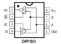
 MAX487芯片引脚图及功能、应用领域详解

 IR2110驱动芯片引脚图及功能、电路图详解

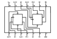
 74LS74是什么芯片 74LS74引脚图及功能表

 CD4511芯片引脚图及功能、电路图解析
