
 5秒后页面跳转

| 是否Rohs认证: | 不符合 | 生命周期: | Obsolete |
| 零件包装代码: | DFP | 包装说明: | DFP, FL56,.4,25 |
| 针数: | 56 | Reach Compliance Code: | not_compliant |
| ECCN代码: | 3A001.A.2.C | HTS代码: | 8542.39.00.01 |
| 风险等级: | 5.92 | 其他特性: | DIRECTION CONTROL; SELECT INPUT FOR MULTIPLEXED TRANSMISSION OF REGISTERED OR REAL TIME DATA |
| 控制类型: | INDEPENDENT CONTROL | 计数方向: | BIDIRECTIONAL |
| 系列: | AC | JESD-30 代码: | R-GDFP-F56 |
| 长度: | 18.288 mm | 负载电容(CL): | 50 pF |
| 逻辑集成电路类型: | REGISTERED BUS TRANSCEIVER | 最大I(ol): | 0.024 A |
| 位数: | 8 | 功能数量: | 2 |
| 端口数量: | 2 | 端子数量: | 56 |
| 最高工作温度: | 125 °C | 最低工作温度: | -55 °C |
| 输出特性: | 3-STATE | 输出极性: | TRUE |
| 封装主体材料: | CERAMIC, GLASS-SEALED | 封装代码: | DFP |
| 封装等效代码: | FL56,.4,25 | 封装形状: | RECTANGULAR |
| 封装形式: | FLATPACK | 峰值回流温度(摄氏度): | NOT SPECIFIED |
| 电源: | 3.3/5 V | Prop。Delay @ Nom-Sup: | 15.7 ns |
| 传播延迟(tpd): | 12.5 ns | 认证状态: | Not Qualified |
| 座面最大高度: | 3.05 mm | 子类别: | Bus Driver/Transceivers |
| 最大供电电压 (Vsup): | 5.5 V | 最小供电电压 (Vsup): | 3 V |
| 标称供电电压 (Vsup): | 5 V | 表面贴装: | YES |
| 技术: | CMOS | 温度等级: | MILITARY |
| 端子形式: | FLAT | 端子节距: | 0.635 mm |
| 端子位置: | DUAL | 处于峰值回流温度下的最长时间: | NOT SPECIFIED |
| 翻译: | N/A | 触发器类型: | POSITIVE EDGE |
| 宽度: | 9.652 mm | Base Number Matches: | 1 |
| 型号 | 品牌 | 描述 | 获取价格 | 数据表 |
| 54AC16646WD | ETC | Dual 8-bit Bus Transceiver |
获取价格 |

|
| 54AC16652 | TI | 16-BIT BUS TRANSCEIVERS AND REGISTERS WITH 3-STATE OUTPUTS |
获取价格 |
|
| 54AC16652_08 | TI | 16-BIT BUS TRANSCEIVERS AND REGISTERS WITH 3-STATE OUTPUTS |
获取价格 |
|
| 54AC16652WD | TI | 16-BIT BUS TRANSCEIVERS AND REGISTERS WITH 3-STATE OUTPUTS |
获取价格 |
|
| 54AC16657WD | ETC | Dual 8-bit Bus Transceiver |
获取价格 |
|
| 54AC16821WD | ETC | Logic IC |
获取价格 |
|
 74LS74是什么芯片 74LS74引脚图及功能表

 CD4511芯片引脚图及功能、电路图解析
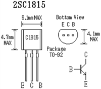 2SC1815三极管参数及引脚图功能详解
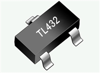 TL432和TL431有什么区别
工作时间:9:00-21:00
CEO邮箱:ceo@jiepei.com
投诉邮箱:tousu@jiepei.com


 浙公网安备 33010502006866号 浙ICP备10014259号-119
营业执照ICP证
浙公网安备 33010502006866号 浙ICP备10014259号-119
营业执照ICP证


