
 5秒后页面跳转

| 是否Rohs认证: | 不符合 | 生命周期: | Obsolete |
| Reach Compliance Code: | unknown | 风险等级: | 5.89 |
| Is Samacsys: | N | 阵列类型: | FRAME |
| 主体宽度: | 7 mm | 主体高度: | 0.87 mm |
| 主体长度或直径: | 7 mm | 外壳: | PLASTIC |
| JESD-609代码: | e0 | 安装特点: | THROUGH HOLE MOUNT |
| 最高工作温度: | 75 °C | 最低工作温度: | -20 °C |
| 光学格式: | 1/1.8 inch | 输出接口类型: | 3-WIRE INTERFACE |
| 输出范围: | 0.40-2.80V | 输出类型: | DIGITAL VOLTAGE |
| 封装形状/形式: | SQUARE | 灵敏度(V / lx.s): | 18 V/lx.s |
| 传感器/换能器类型: | IMAGE SENSOR,CCD | 最大供电电压: | 5.25 V |
| 最小供电电压: | 3 V | 表面贴装: | NO |
| 端子面层: | Tin/Lead (Sn/Pb) | 端接类型: | SOLDER |
| Base Number Matches: | 1 |
| 型号 | 品牌 | 描述 | 获取价格 | 数据表 |
| CXD3606R | SONY | Timing Generator for Frame Readout CCD Image Sensor |
获取价格 |

|
| CXD3607R | SONY | Timing Generator for Progressive Scan CCD Image Sensor |
获取价格 |
|
| CXD3609R | SONY | Timing Generator for Progressive Scan CCD Image Sensor |
获取价格 |
|
| CXD3611R | SONY | Timing Generator for Progressive Scan CCD Image Sensor |
获取价格 |
|
| CXD3615R | SONY | Timing Generator for Frame Readout CCD Image Sensor |
获取价格 |
|
| CXD3619R | SONY | Timing Generator for Frame Readout CCD Image Sensor |
获取价格 |
|
 74LS74是什么芯片 74LS74引脚图及功能表

 CD4511芯片引脚图及功能、电路图解析
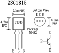 2SC1815三极管参数及引脚图功能详解
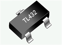 TL432和TL431有什么区别
工作时间:9:00-21:00
CEO邮箱:ceo@jiepei.com
投诉邮箱:tousu@jiepei.com


 浙公网安备 33010502006866号 浙ICP备10014259号-119
营业执照ICP证
浙公网安备 33010502006866号 浙ICP备10014259号-119
营业执照ICP证


