
 5秒后页面跳转

| 是否无铅: | 含铅 | 是否Rohs认证: | 不符合 |
| 生命周期: | Active | Reach Compliance Code: | not_compliant |
| ECCN代码: | EAR99 | HTS代码: | 8542.39.00.01 |
| Factory Lead Time: | 18 weeks | 风险等级: | 2.26 |
| 模拟集成电路 - 其他类型: | SPST | 湿度敏感等级: | 1 |
| 信道数量: | 1 | 功能数量: | 2 |
| 端子数量: | 14 | 封装主体材料: | CERAMIC, GLASS-SEALED |
| 封装形式: | IN-LINE | 峰值回流温度(摄氏度): | 240 |
| 技术: | CMOS | 端子位置: | DUAL |
| 处于峰值回流温度下的最长时间: | 20 | Base Number Matches: | 1 |
| 型号 | 品牌 | 描述 | 获取价格 | 数据表 |
| DG200AAK/HR | ETC | SPST Analog Switch |
获取价格 |

|
| DG200AAL | ETC | SPST Analog Switch |
获取价格 |
|
| DG200AAL/883 | ETC | SPST Analog Switch |
获取价格 |
|
| DG200AAL/883B | MAXIM | SPST, |
获取价格 |
|
| DG200AAP/883 | VISHAY | IC DUAL 1-CHANNEL, SGL POLE SGL THROW SWITCH, CDIP14, SIDEBRAZED, CERAMIC, DIP-14, Multipl |
获取价格 |
|
| DG200ABA | MAXIM | Dual Monolithic SPST CMOS Analog Switch |
获取价格 |
|
 74LS74是什么芯片 74LS74引脚图及功能表

 CD4511芯片引脚图及功能、电路图解析
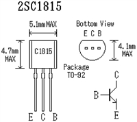 2SC1815三极管参数及引脚图功能详解
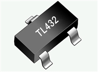 TL432和TL431有什么区别
工作时间:9:00-21:00
CEO邮箱:ceo@jiepei.com
投诉邮箱:tousu@jiepei.com


 浙公网安备 33010502006866号 浙ICP备10014259号-119
营业执照ICP证
浙公网安备 33010502006866号 浙ICP备10014259号-119
营业执照ICP证


