Document Number: MC33903_4_5
Rev. 6.0, 4/2011
Freescale Semiconductor
Technical Data
SBC Gen2 with CAN High Speed
and LIN Interface
33903/
33903/4/5
The 33903/4/5 is the second generation family of the System Basis
Chip (SBC). It combines several features and enhances present
module designs. The device works as an advanced power
management unit for the MCU with additional integrated circuits such
as sensors, and CAN transceivers. It has a built-in enhanced high
speed CAN interface (ISO11898-2 and -5) with local and bus failure
diagnostics, protection, and Fail Safe Operation Modes. The SBC may
include zero, one or two LIN 2.1 interfaces with LIN output pin switches.
It includes up to four Wake-Up input pins that can also be configured as
output drivers for flexibility.
SYSTEM BASIS CHIP
This device implements multiple Low Power (LP) Modes, with very
low-current consumption. In addition, the device is part of a family
concept where pin compatibility adds versatility to module design.
EK Suffix (Pb-Free)
98ASA10506D
54-PIN SOIC
EK Suffix (Pb-Free)
98ASA10556D
32-PIN SOIC
The 33903/4/5 also implements an innovative and advanced fail-safe
state machine and concept solution.
ORDERING INFORMATION
Features
See Table of Contents 2
• Voltage regulator for MCU, 5.0 or 3.3 V, part number selectable, with
possibility of usage external PNP to extend current capability and
share power dissipation
• Voltage, current, and temperature protection
• Extremely low quiescent current in (LP) Modes
• Fully-protected embedded 5.0 V regulator for the CAN driver
• Multiple under-voltage detections to address various MCU
specifications and system operation modes (i.e. cranking)
• Auxiliary 5.0 or 3.3 V SPI configurable regulator, for additional ICs,
with over-current detection and under-voltage protection
• MUX (except 33903) output pin for device internal analog signal
monitoring and power supply monitoring
• Advanced SPI, MCU, ECU power supply, and critical pins
diagnostics and monitoring.
• Multiple Wake-Up sources in (LP) Modes: CAN or LIN bus, I/O
transition, automatic timer, SPI message, and VDD over-current
detection.
• ISO11898-5 high speed CAN interface compatibility for baud rates of
40 kb/s to 1.0 Mb/s
Freescale Semiconductor, Inc. reserves the right to change the detail specifications,
as may be required, to permit improvements in the design of its products.
© Freescale Semiconductor, Inc., 2010 - 2011. All rights reserved.


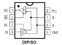
 MAX487芯片引脚图及功能、应用领域详解

 IR2110驱动芯片引脚图及功能、电路图详解

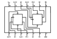
 74LS74是什么芯片 74LS74引脚图及功能表

 CD4511芯片引脚图及功能、电路图解析
