
 5秒后页面跳转

| 是否Rohs认证: | 不符合 | 生命周期: | Obsolete |
| 零件包装代码: | QFP | 包装说明: | TQFP-32 |
| 针数: | 32 | Reach Compliance Code: | compliant |
| HTS代码: | 8542.39.00.01 | 风险等级: | 5.92 |
| Is Samacsys: | N | 系列: | 9946 |
| 输入调节: | MUX | JESD-30 代码: | S-PQFP-G32 |
| 长度: | 7 mm | 逻辑集成电路类型: | LOW SKEW CLOCK DRIVER |
| 最大I(ol): | 0.02 A | 功能数量: | 1 |
| 反相输出次数: | 端子数量: | 32 | |
| 实输出次数: | 10 | 最高工作温度: | 85 °C |
| 最低工作温度: | -40 °C | 输出特性: | 3-STATE |
| 封装主体材料: | PLASTIC/EPOXY | 封装代码: | TQFP |
| 封装等效代码: | TQFP32,.35SQ,32 | 封装形状: | SQUARE |
| 封装形式: | FLATPACK, THIN PROFILE | 峰值回流温度(摄氏度): | NOT SPECIFIED |
| 电源: | 3.3 V | Prop。Delay @ Nom-Sup: | 11.5 ns |
| 传播延迟(tpd): | 11.5 ns | 认证状态: | Not Qualified |
| Same Edge Skew-Max(tskwd): | 0.25 ns | 座面最大高度: | 1.2 mm |
| 子类别: | Clock Drivers | 最大供电电压 (Vsup): | 3.63 V |
| 最小供电电压 (Vsup): | 2.97 V | 标称供电电压 (Vsup): | 3.3 V |
| 表面贴装: | YES | 温度等级: | INDUSTRIAL |
| 端子形式: | GULL WING | 端子节距: | 0.8 mm |
| 端子位置: | QUAD | 处于峰值回流温度下的最长时间: | NOT SPECIFIED |
| 宽度: | 7 mm | 最小 fmax: | 160 MHz |
| Base Number Matches: | 1 |
| 型号 | 品牌 | 描述 | 获取价格 | 数据表 |
| B9946CA | CYPRESS | 3.3V, 160-MHz, 1:10 Clock Distribution Buffer |
获取价格 |

|
| B9947 | CYPRESS | 3.3V, 160-MHz, 1:9 Clock Distribution Buffer |
获取价格 |
|
| B9947CA | CYPRESS | 3.3V, 160-MHz, 1:9 Clock Distribution Buffer |
获取价格 |
|
| B9948 | CYPRESS | 3.3V, 160-MHz, 1:12 Clock Distribution Buffer |
获取价格 |
|
| B9948CA | ETC | TWELVE DISTRIBUTED-OUTPUT CLOCK DRIVER|TQFP|32PIN|PLASTIC |
获取价格 |
|
| B9948L | CYPRESS | 2.5V/3.3V, 160-MHz, 1:12 Clock Distribution Buffer |
获取价格 |
|
 74LS74是什么芯片 74LS74引脚图及功能表

 CD4511芯片引脚图及功能、电路图解析
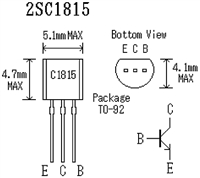 2SC1815三极管参数及引脚图功能详解
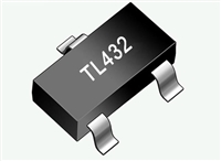 TL432和TL431有什么区别
工作时间:9:00-21:00
CEO邮箱:ceo@jiepei.com
投诉邮箱:tousu@jiepei.com


 浙公网安备 33010502006866号 浙ICP备10014259号-119
营业执照ICP证
浙公网安备 33010502006866号 浙ICP备10014259号-119
营业执照ICP证


