CY7C199
32K x 8 Static RAM
is provided by an active LOW Chip Enable (CE) and active
LOW Output Enable (OE) and three-state drivers. This device
has an automatic power-down feature, reducing the power
consumption by 81% when deselected. The CY7C199 is in the
standard 300-mil-wide DIP, SOJ, and LCC packages.
Features
• High speed
— 10 ns
• Fast tDOE
An active LOW Write Enable signal (WE) controls the
writing/reading operation of the memory. When CE and WE
inputs are both LOW, data on the eight data input/output pins
(I/O0 through I/O7) is written into the memory location
addressed by the address present on the address pins (A0
through A14). Reading the device is accomplished by selecting
the device and enabling the outputs, CE and OE active LOW,
while WE remains inactive or HIGH. Under these conditions,
the contents of the location addressed by the information on
address pins are present on the eight data input/output pins.
• CMOS for optimum speed/power
• Low active power
— 467 mW (max, 12 ns “L” version)
• Low standby power
— 0.275 mW (max, “L” version)
• 2V data retention (“L” version only)
• Easy memory expansion with CE and OE features
• TTL-compatible inputs and outputs
• Automatic power-down when deselected
The input/output pins remain in a high-impedance state unless
the chip is selected, outputs are enabled, and Write Enable
(WE) is HIGH. A die coat is used to improve alpha immunity.
Functional Description
The CY7C199 is a high-performance CMOS static RAM
organized as 32,768 words by 8 bits. Easy memory expansion
Logic Block Diagram
Pin Configurations
DIP / SOJ / SOIC
LCC
Top View
Top View
A
A
V
CC
28
27
26
1
2
3
4
5
6
5
WE
6
3
2 1 2827
26
A
A
A
4
7
4
A
4
A
8
8
A
3
25
24
5
6
7
8
25
24
23
22
21
20
19
18
A
A
9
3
A
9
A
2
A
1
A
A
10
11
12
13
14
2
A
10
A
11
23
22
A
A
A
A
A
1
OE
7
OE
9
I/O
I/O
I/O
I/O
I/O
I/O
I/O
A
A
A
I/O
I/O
I/O
A
21
20
19
18
17
16
15
A
12
13
14
0
0
1
2
3
4
5
6
8
9
10
11
12
13
0
10
11
12
CE
I/O
I/O
INPUT BUFFER
CE
I/O
I/O
I/O
I/O
I/O
0
7
6
7
1
A
0
0
1
2
6
5
4
1314151617
A
1
A
2
I/O
I/O
A
GND
3
14
3
A
4
1024 x 32 x 8
ARRAY
22
A
OE
A
5
21
A
0
A
23
24
1
6
A
20
CE
I/O
I/O
A
A
A
7
A
2
3
4
19
18
17
16
7
6
8
A
25
26
27
28
1
9
I/O
I/O
I/O
GND
I/O
5
4
3
TSOP I
Top View
(not to scale)
WE
V
CC
A
15
14
13
CE
WE
5
6
7
POWER
DOWN
COLUMN
DECODER
A
A
A
2
3
2
12
11
I/O
I/O
A
1
0
14
I/O
4
5
7
8
9
OE
A
10
9
A
6
7
10
A
A
13
12
A
11
8
Selection Guide
7C199 7C199
7C199 7C199 7C199 7C199 7C199 7C199
-8
-10
10
-12
12
-15
15
-20
20
-25
25
-35
35
-45
45
Unit
ns
Maximum Access Time
8
Maximum Operating Current
120
110
90
0.5
0.05
160
90
10
155
90
10
150
90
10
150
80
10
140
70
10
140
mA
L
L
Maximum CMOS Standby Current
0.5
10
mA
0.05
0.05
0.05
0.05
0.05
Shaded area contains advance information.
Cypress Semiconductor Corporation
Document #: 38-05160 Rev. *A
•
3901 North First Street
•
San Jose, CA 95134
•
408-943-2600
Revised January 7, 2003

 5秒后页面跳转


 74LS74是什么芯片 74LS74引脚图及功能表

 CD4511芯片引脚图及功能、电路图解析
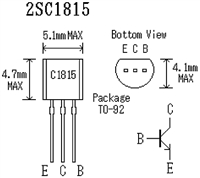 2SC1815三极管参数及引脚图功能详解
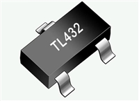 TL432和TL431有什么区别


 浙公网安备 33010502006866号 浙ICP备10014259号-119
营业执照ICP证
浙公网安备 33010502006866号 浙ICP备10014259号-119
营业执照ICP证


