
 5秒后页面跳转

| 生命周期: | Obsolete | 零件包装代码: | QFJ |
| 包装说明: | QCCN, | 针数: | 32 |
| Reach Compliance Code: | unknown | ECCN代码: | EAR99 |
| HTS代码: | 8542.32.00.71 | 风险等级: | 5.84 |
| 最长访问时间: | 10 ns | 其他特性: | RETRANSMIT |
| 周期时间: | 15 ns | 长度: | 13.97 mm |
| 内存密度: | 294912 bit | 内存宽度: | 9 |
| 功能数量: | 1 | 字数: | 32768 words |
| 字数代码: | 32000 | 工作模式: | SYNCHRONOUS |
| 最高工作温度: | 125 °C | 最低工作温度: | -55 °C |
| 组织: | 32KX9 | 可输出: | YES |
| 封装主体材料: | CERAMIC, METAL-SEALED COFIRED | 封装代码: | QCCN |
| 封装形式: | CHIP CARRIER | 并行/串行: | PARALLEL |
| 认证状态: | Not Qualified | 筛选级别: | MIL-PRF-38535 Class Q |
| 座面最大高度: | 2.286 mm | 最大供电电压 (Vsup): | 5.5 V |
| 最小供电电压 (Vsup): | 4.5 V | 标称供电电压 (Vsup): | 5 V |
| 表面贴装: | YES | 技术: | CMOS |
| 温度等级: | MILITARY | 端子形式: | NO LEAD |
| 端子节距: | 1.27 mm | 端子位置: | QUAD |
| 宽度: | 11.43 mm | Base Number Matches: | 1 |
| 型号 | 品牌 | 描述 | 获取价格 | 数据表 |
| 5962-9736101QYX | CYPRESS | FIFO, 32KX9, 10ns, Synchronous, CMOS, CQCC32, CERAMIC, LCC-32 |
获取价格 |

|
| 5962-9745801QEA | TI | TTL/H/L SERIES, SYN POSITIVE EDGE TRIGGERED 4-BIT UP BINARY COUNTER, CDIP16, CERAMIC, DIP- |
获取价格 |
|
| 5962-9745801QEX | TI | TTL/H/L SERIES, SYN POSITIVE EDGE TRIGGERED 4-BIT UP BINARY COUNTER, CDIP16, CERAMIC, DIP- |
获取价格 |
|
| 5962-9745801QFA | TI | IC TTL/H/L SERIES, SYN POSITIVE EDGE TRIGGERED 4-BIT UP BINARY COUNTER, CDFP16, CERAMIC, D |
获取价格 |
|
| 5962-9750401MXA | ETC | Digital Filter |
获取价格 |
|
| 5962-9750401MXC | ETC | Digital Filter |
获取价格 |
|
 74LS74是什么芯片 74LS74引脚图及功能表

 CD4511芯片引脚图及功能、电路图解析
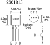 2SC1815三极管参数及引脚图功能详解
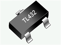 TL432和TL431有什么区别
工作时间:9:00-21:00
CEO邮箱:ceo@jiepei.com
投诉邮箱:tousu@jiepei.com


 浙公网安备 33010502006866号 浙ICP备10014259号-119
营业执照ICP证
浙公网安备 33010502006866号 浙ICP备10014259号-119
营业执照ICP证


