5895
8-BIT SERIAL-INPUT,
LATCHED DRIVERS
5895
BiMOS II 8-BIT SERIAL INPUT,
LATCHED SOURCE DRIVERS
The UCN5895A, UCN5895EP, and A5895SLW BiMOS II serial-
input, latched source drivers are designed for applications emphasiz-
ing low output saturation voltages and currents to -250 mA per output.
These smart high-side octal, driver ICs merge an 8-bit CMOS shift
register, associated CMOS latches, and CMOS control logic (strobe
and output enable) with medium current emitter-follower (sourcing)
outputs. Typical applications include incandescent or LED displays
(both directly driven and multiplexed), non-impact (i.e., thermal)
printers, relays, and solenoids.
UCN5895A
SERIAL
DATA OUT
16
15
GROUND
CLOCK
1
2
3
4
LOGIC
SUPPLY
V
CLK
ST
DD
SHIFT
REGISTER
OUTPUT
ENABLE
SERIAL
DATA IN
OE 14
LOAD
SUPPLY
V
13
STROBE
BB
LATCHES
Each device is suitable for high-side applications to -250 mA per
channel. The maximum supply voltage is 50 V and a minimum output
sustaining voltage rating of 35 V for inductive load applications. Under
normal operating conditions, the UCN5895A and UCN5895EP are
capable of providing -120 mA (8 outputs continuous and simultaneous)
at +65°C with a logic supply of 5 V. Similar devices, with higher output
current ratings, are the UCN5890A and UCN5891A.
12 OUT
11 OUT
OUT
1
5
6
8
7
6
5
OUT
2
OUT
OUT
OUT
3
10
9
7
8
OUT
4
BiMOS II devices can operate at greatly improved data-input rates.
With a 5 V supply, they will typically operate at better than 5 MHz.
At 12 V, significantly higher speeds are obtained.
Dwg. PP-026-2A
Note the UCN5895A (DIP) and the A5895SLW
(SOIC) are electrically identical and share a common
terminal number assignment.
The CMOS inputs provide for minimum loading and are compatible
with standard CMOS, PMOS, and NMOS circuits. TTL or DTL circuits
may require the use of appropriate pull-up resistors to ensure a proper
input-logic high. A CMOS serial data output allows cascading these
devices in multiple drive-line applications required by many dot matrix,
alphanumeric, and bar graph displays.
ABSOLUTE MAXIMUM RATINGS
at T = +25°C
A
Output Voltage, VOUT . . . . . . . . . . . . . . 50 V
Logic Supply Voltage Range,
These devices are rated for continuous operation over the tem-
perature range of -20°C to +85°C. Because of limitations on package
power dissipation, the simultaneous operation of all output drivers may
require a reduction in duty cycle. The UCN5895A is supplied in a
standard 16-pin dual in-line plastic package with a copper lead frame
for increased allowable package power dissipation. The UCN5895EP
is supplied in a 20-lead plastic leaded chip carrier for minimum area,
surface-mount applications. The A5895SLW is supplied in a 16-lead
wide-body plastic SOIC.
V
DD . . . . . . . . . . . . . . . . . . 4.5 V to 12 V
Driver Supply Voltage Range,
BB . . . . . . . . . . . . . . . . . . 5.0 V to 50 V
V
Input Voltage Range,
VIN . . . . . . . . . . . -0.3 V to VDD + 0.3 V
Continuous Output Current,
IOUT . . . . . . . . . . . . . . . . . . . . . -250 mA
Allowable Package Power Dissipation,
PD . . . . . . . . . . . . . . . . . . . . See Graph
Operating Temperature Range,
TA . . . . . . . . . . . . . . . . . -20°C to +85°C
Storage Temperature Range,
FEATURES
■ Low Output-Saturation Voltage
■ Source Outputs to 50 V
■ Output Current to -250 mA
■ To 3.3 MHz Data-lnput Rate
■ Low-Power CMOS Logic & Latches
TS . . . . . . . . . . . . . . . . -55°C to +150°C
Caution: CMOS devices have input-static
protection, but are susceptible to damage when
exposed to extremely high static electrical
charges.
Always order by complete part number, e.g., UCN5895A .

 5秒后页面跳转


 74LS74是什么芯片 74LS74引脚图及功能表

 CD4511芯片引脚图及功能、电路图解析
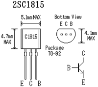 2SC1815三极管参数及引脚图功能详解
 TL432和TL431有什么区别


 浙公网安备 33010502006866号 浙ICP备10014259号-119
营业执照ICP证
浙公网安备 33010502006866号 浙ICP备10014259号-119
营业执照ICP证


