DC to 2.0 GHz
Multiplier
ADL5391
FUNCTIONAL BLOCK DIAGRAM
FEATURES
YMNS YPLS
GADJ
Ultrafast symmetric multiplier
Function: VW = α × (VX × VY)/1 V + VZ
Unique design ensures absolute XY-symmetry
Identical X and Y amplitude/timing responses
Adjustable gain scaling, α
XPLS
XMNS
ZMNS
ZPLS
WPLS
DC-coupled throughout, 3 dB bandwidth of 2 GHz
Fully differential inputs, may be used single ended
Low noise, high linearity
ENBL
VMID
WMNS
ADL5391
W = αXY/1V+Z
Accurate, temperature stable gain scaling
Single-supply operation (4.5 V to 5.5 V @ 130 mA)
Low current power-down mode
COMM VPOS
Figure 1.
16-lead LFCSP
APPLICATIONS
Wideband multiplication and summing
High frequency analog modulation
Adaptive antennas (diversity/phased array)
Square-law detectors and true rms detectors
Accurate polynomial function synthesis
DC capable VGA with very fast control
GENERAL DESCRIPTION
are ac-coupled, their nominal voltage will be VPOS/±. These input
interfaces each present a differential 500 Ω input impedance up to
approximately 700 MHz, decreasing to 50 Ω at ± GHz. The gain
scaling input, GADJ, can be used for fine adjustment of the gain
scaling constant (α) about unity.
The ADL5391 draws on three decades of experience in
advanced analog multiplier products. It provides the same
general mathematical function that has been field proven to
provide an exceptional degree of versatility in function synthesis.
V
W = α × (VX × VY)/ 1 V + VZ
The differential output can swing ±± V about the VPOS/±
common-mode and can be taken in a single-ended fashion as
well. The output common mode is designed to interface directly
to the inputs of another ADL5391. Light dc loads can be ground
referenced; however, ac-coupling of the outputs is recommended
for heavy loads.
The most significant advance in the ADL5391 is the use of a
new multiplier core architecture, which differs markedly from
the conventional form that has been in use since 1970. The
conventional structure that employs a current mode, translinear
core is fundamentally asymmetric with respect to the X and Y
inputs, leading to relative amplitude and timing misalignments
that are problematic at high frequencies. The new multiplier
core eliminates these misalignments by offering symmetric
signal paths for both X and Y inputs. The Z input allows a signal
to be added directly to the output. This can be used to cancel a
carrier or to apply a static offset voltage.
The ENBL pin allows the ADL5391 to be disabled quickly to a
standby mode. It operates off supply voltages from 4.5 V to
5.5 V while consuming approximately 130 mA.
The ADL5391 is fabricated on Analog Devices proprietary, high
performance, 65 GHz, SOI complementary, SiGe bipolar IC
process. It is available in a 16-lead, Pb-free, LFCSP and operates
over a −40°C to +85°C temperature range. Evaluation boards
are available.
The fully differential X, Y, and Z input interfaces are operational
over a ±± V range, and they can be used in single-ended fashion.
The user can apply a common mode at these inputs to vary
from the internally set VPOS/± down to ground. If these inputs
Rev. 0
Information furnished by Analog Devices is believed to be accurate and reliable. However, no
responsibility is assumed by Analog Devices for its use, nor for any infringements of patents or other
rights of third parties that may result from its use. Specifications subject to change without notice. No
license is granted by implication or otherwise under any patent or patent rights of Analog Devices.
Trademarks and registeredtrademarks arethe property of their respective owners.
One Technology Way, P.O. Box 9106, Norwood, MA 02062-9106, U.S.A.
Tel: 781.329.4700
Fax: 781.461.3113
www.analog.com
©2006 Analog Devices, Inc. All rights reserved.


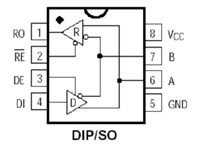
 MAX487芯片引脚图及功能、应用领域详解

 IR2110驱动芯片引脚图及功能、电路图详解

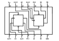
 74LS74是什么芯片 74LS74引脚图及功能表

 CD4511芯片引脚图及功能、电路图解析
