
 5秒后页面跳转

| 是否无铅: | 含铅 | 是否Rohs认证: | 符合 |
| 生命周期: | Active | 零件包装代码: | QFN |
| 包装说明: | HVQCCN, | 针数: | 32 |
| Reach Compliance Code: | compliant | ECCN代码: | 5A991.B |
| HTS代码: | 8542.39.00.01 | 风险等级: | 1.65 |
| Samacsys Confidence: | Samacsys Status: | Released | |
| Schematic Symbol: | https://componentsearchengine.com/symbol.php?partID=577635 | PCB Footprint: | https://componentsearchengine.com/footprint.php?partID=577635 |
| Samacsys PartID: | 577635 | Samacsys Image: | https://componentsearchengine.com/Images/9/ADL5240ACPZ-R7.jpg |
| Samacsys Thumbnail Image: | https://componentsearchengine.com/Thumbnails/1/ADL5240ACPZ-R7.jpg | Samacsys Pin Count: | 33 |
| Samacsys Part Category: | Integrated Circuit | Samacsys Package Category: | Other |
| Samacsys Footprint Name: | QFN50P500X500X100-33N | Samacsys Released Date: | 2017-01-10 13:33:33 |
| Is Samacsys: | N | JESD-30 代码: | S-XQCC-N32 |
| JESD-609代码: | e3 | 长度: | 5 mm |
| 湿度敏感等级: | 3 | 功能数量: | 1 |
| 端子数量: | 32 | 最高工作温度: | 85 °C |
| 最低工作温度: | -40 °C | 封装主体材料: | UNSPECIFIED |
| 封装代码: | HVQCCN | 封装形状: | SQUARE |
| 封装形式: | CHIP CARRIER, HEAT SINK/SLUG, VERY THIN PROFILE | 峰值回流温度(摄氏度): | NOT SPECIFIED |
| 认证状态: | Not Qualified | 座面最大高度: | 1 mm |
| 标称供电电压: | 5 V | 表面贴装: | YES |
| 电信集成电路类型: | TELECOM CIRCUIT | 温度等级: | INDUSTRIAL |
| 端子面层: | Matte Tin (Sn) | 端子形式: | NO LEAD |
| 端子节距: | 0.5 mm | 端子位置: | QUAD |
| 处于峰值回流温度下的最长时间: | NOT SPECIFIED | 宽度: | 5 mm |
| Base Number Matches: | 1 |
| 型号 | 品牌 | 描述 | 获取价格 | 数据表 |
| ADL5240-EVALZ | ADI | 100 MHz to 4000 MHz RF/IF Digitally Controlled VGA |
获取价格 |

|
| ADL5243 | ADI | 100 MHz to 4000 MHz RF/IF Digitally Controlled VGA |
获取价格 |
|
| ADL5243ACPZ-R7 | ADI | 100 MHz to 4000 MHz RF/IF Digitally Controlled VGA |
获取价格 |
|
| ADL5243-EVALZ | ADI | 100 MHz to 4000 MHz RF/IF Digitally Controlled VGA |
获取价格 |
|
| ADL5246 | ADI | 3 GHz Variable Gain LNA with Integrated ½ W |
获取价格 |
|
| ADL5246ACPZN-R7 | ADI | 3 GHz Variable Gain LNA with Integrated ½ W D |
获取价格 |
|
 74LS74是什么芯片 74LS74引脚图及功能表

 CD4511芯片引脚图及功能、电路图解析
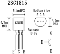 2SC1815三极管参数及引脚图功能详解
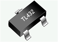 TL432和TL431有什么区别
工作时间:9:00-21:00
CEO邮箱:ceo@jiepei.com
投诉邮箱:tousu@jiepei.com


 浙公网安备 33010502006866号 浙ICP备10014259号-119
营业执照ICP证
浙公网安备 33010502006866号 浙ICP备10014259号-119
营业执照ICP证


