CDMA 3 V Receiver IF Subsystem
with Integrated Voltage Regulator
a
AD6121
FEATURES
GENERAL DESCRIPTION
Fully Compliant with IS98A and PCS Specifications
CDMA, W-CDMA, AMPS, and TACS Operation
Linear IF Amplifier
5.9 dB Noise Figure
–47.5 dB to +47 dB Linear-in-dB Gain Control
Quadrature Demodulator
The AD6121 is a low power receiver IF subsystem specifically
designed for CDMA applications. It consists of high dynamic
range IF amplifiers with voltage controlled gain, a divide-by-two
quadrature generator, an I and Q demodulator, and a power-
down control input. An integral low dropout regulator allows
operation from battery voltages from 2.9 V to 4.2 V.
Demodulates IFs from 50 MHz to 350 MHz
Integral Low Dropout Regulator
200 mV Voltage Drop
Accepts 2.9 V to 4.2 V Input from Battery
Low Power
The gain control input accepts an external gain control voltage
input from a DAC. It provides 94.5 dB of gain control with a
nominal 52.5 dB/V scale factor when using an internal voltage
reference. The gain control interface reference input can be
connected to either the internal reference or an external reference.
10 mA at Midgain
The I and Q demodulator provides differential quadrature base-
band outputs to interface with CDMA baseband converters. A
divide-by-two quadrature generator followed by dual polyphase
filters ensures maximum 2.5° quadrature accuracy.
<1 A Sleep Mode Operation
Companion Transmitter IF Chip Available (AD6122)
APPLICATIONS
CDMA, W-CDMA, AMPS, and TACS Operation
QPSK Receivers
The AD6121 IF Subsystem is fabricated using a 25 GHz ft
BiCMOS silicon process and is packaged in a 28-lead SSOP
and a 32-leadless LPCC chip scale package (5 mm × 5 mm).
FUNCTIONAL BLOCK DIAGRAM
ROOFING
FILTER
IF
DEMODULATOR
INPUT
OUTPUT
IOUT
CDMA
INPUT
IOUT
IF AMPLIFIERS
I
LOCAL
OSCILLATOR
INPUT
2
Q
QOUT
AD6121
FM
INPUT
QOUT
QUADRATURE DEMODULATOR
INPUT STAGE
VPOS
LOW
DROPOUT
REGULATOR
VREG
PTAT
TEMPERATURE
COMPENSATION
GAIN CONTROL
SCALE FACTOR
POWER- POWER-
DOWN 2 DOWN 1
CONTROL REFERENCE
CDMA/FM
SELECT
GAIN
CONTROL
VOLTAGE
INPUT
GAIN
1.23V
VOLTAGE
REFERENCE
INPUT
OUTPUT
REV. B
Information furnished by Analog Devices is believed to be accurate and
reliable. However, no responsibility is assumed by Analog Devices for its
use, nor for any infringements of patents or other rights of third parties
which may result from its use. No license is granted by implication or
otherwise under any patent or patent rights of Analog Devices.
One Technology Way, P.O. Box 9106, Norwood, MA 02062-9106, U.S.A.
Tel: 781/329-4700
Fax: 781/326-8703
World Wide Web Site: http://www.analog.com
© Analog Devices, Inc., 2000


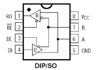
 MAX487芯片引脚图及功能、应用领域详解

 IR2110驱动芯片引脚图及功能、电路图详解

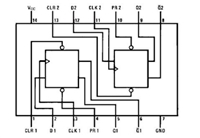
 74LS74是什么芯片 74LS74引脚图及功能表

 CD4511芯片引脚图及功能、电路图解析
