
 5秒后页面跳转

| 型号 | 品牌 | 描述 | 获取价格 | 数据表 |
| 27L512-15 | Macronix | 512K-BIT [64K x 8] CMOS EPROM |
获取价格 |

|
| 27L512-20 | Macronix | 512K-BIT [64K x 8] CMOS EPROM |
获取价格 |
|
| 27L512-25 | Macronix | 512K-BIT [64K x 8] CMOS EPROM |
获取价格 |
|
| 27LC128-12EL | MICROCHIP | 128K (16K x 8) CMOS EPROM |
获取价格 |
|
| 27LC128-12EP | MICROCHIP | 128K (16K x 8) CMOS EPROM |
获取价格 |
|
| 27LC128-12ESO | MICROCHIP | 128K (16K x 8) CMOS EPROM |
获取价格 |
|
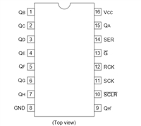 74HC595移位寄存器芯片:参数深入解析与应用实践指南

 AO3401场效应管参数、引脚图、应用原理图
 BT131可控硅参数及引脚图、工作原理详解
 74LS32芯片参数、引脚图及功能真值表
工作时间:9:00-21:00
CEO邮箱:ceo@jiepei.com
投诉邮箱:tousu@jiepei.com


 浙公网安备 33010502006866号 浙ICP备10014259号-119
营业执照ICP证
浙公网安备 33010502006866号 浙ICP备10014259号-119
营业执照ICP证


